Download
1 / 39
390 likes | 559 Views
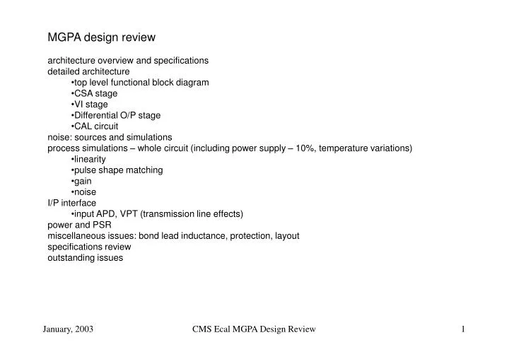
MGPA design review architecture overview and specifications detailed architecture top level functional block diagram CSA stage VI stage Differential O/P stage CAL circuit noise: sources and simulations

E N D
MGPA design review • architecture overview and specifications • detailed architecture • top level functional block diagram • CSA stage • VI stage • Differential O/P stage • CAL circuit • noise: sources and simulations • process simulations – whole circuit (including power supply – 10%, temperature variations) • linearity • pulse shape matching • gain • noise • I/P interface • input APD, VPT (transmission line effects) • power and PSR • miscellaneous issues: bond lead inductance, protection, layout • specifications review • outstanding issues CMS Ecal MGPA Design Review
MGPA specifications Vpk-25ns Vpk Vpk-25ns/Vpk matches to 1% across gain ranges CMS Ecal MGPA Design Review
MGPA – architecture overview V/I gain resistors external components define CR and CSA gain diff. O/P external components define RC offset adjust offset & CAL pulse generation I2C interface CMS Ecal MGPA Design Review
CSA I/P stage conventional folded cascode maximise use of available dynamic range resistor to VDD -> I/P device Vs ~ 1V => I/P and O/P as close as poss. to VSS note output -> PMOS source followers with ~0.5V VGS ext. components define gain and O/P decay time (40 ns) choose to suit barrel/endcap Cpf/Rpf = 33pF/1.3k (barrel) or 10pf/4k (endcap) => max signal accommodated (~ 1V) with min. pile-up input device dimensions big gm needed for low O/P risetime (Cdet~200pF) 30,000/0.36 -> Cgs ~60 pF, gm~.3A/V bias current magnitudes (externally defined) for big I/P device gm (see above) slew rate at output node bias transistor dimensions avoid minimum length keep gm low (noise) but need low Vdsat CMS Ecal MGPA Design Review
CSA O/P simulation (barrel case) nominal process parameters Cpf/Rpf = 33pF/1.2k input capacitance 200 pF signal injected at 25 ns 0 -> 60 pC in 2pC steps 10 ns arrival time to simulate scintillation decay time resulting pulse peaks at 47 ns (22ns injection -> pk) ~ 1.1 Volt max amplitude swing CMS Ecal MGPA Design Review
CSA O/P simulation (end-cap case) Cpf/Rpf = 10pF/4k input capacitance 50 pF signal injected at 25 ns 0 -> 16 pC in 1pC steps 10 ns arrival time to simulate scintillation decay time resulting pulse peaks at 48 ns => 23ns injection -> pk ~ 1.0 Volt max amplitude swing CSA O/P pulse shape ~ independent of whether barrel or endcap CMS Ecal MGPA Design Review
VI stage design choices governed by: linearity, noise considerations, supply current requirements (not excessive), need to produce current output (high O/P impedance) to drive diff. O/P stage Rgain gives good linearity acceptable noise (later) s.f. and cascode currents all derived from one current source cascode gate voltage derived from preamp I/P ensures minimum DC voltage across Rgain s.f. and cascode widths and drain currents for large gm (note Rgain values relatively small) IDS different for different gain stages chosen to get linearity within spec. trade-off linearity/power RC coupled (external) CMS Ecal MGPA Design Review
2.2V source follower O/P cascode O/P VI stage simulation waveforms (nominal process parameters) low gain channel signal: 0 -> 60 pC in 6 pC steps 1.1V cascode I/P CMS Ecal MGPA Design Review
Differential O/P stage single ended current in -> differential current out ADC I/P signal range: +/- 0.45 V around Vcm (1.25V) O/P RC termination sets shaping time const. 200 ohms compromise between “low-ish” O/P impedance and DC quiescent current 40 nsec requires 100 pF differential (2.5 pF/nsec) or 200 pF each O/P to Vcm (5 pF/nsec) programmable offset adjust to each channel CMS Ecal MGPA Design Review
Lowest gain channel – differential O/P stage signals signals: 0 – 60 pC, 2 pC steps VCM = 1.25 V CMS Ecal MGPA Design Review
Higher gain channels – saturation effects (still0 – 60 pC, 2 pC steps) middle gain range highest gain range CMS Ecal MGPA Design Review
MGPA output: (out+) – (out-) 0 – 60 pC, 2 pC steps highest (red) and mid (blue) gain ranges saturate lowest (green) well-behaved CMS Ecal MGPA Design Review
CAL circuit CMS Ecal MGPA Design Review
CAL circuit simulation MGPA I/P 10pF DAC value e.g. 100mV Rtc:0 ->10W 10k Rtc 1nF external components Highest gain channel O/P for 1 pC input signal Can use Rtc to simulate real signal risetime CMS Ecal MGPA Design Review
Noise Rpf diff. O/P gain stage transconductance gain stage vRpf2 CI Cpf iCFET2 s.f. RG RI vFET2 CIN charge amp. iRG2 VCM ENC due to charge amp. noise sources: Rpf : note: Rpf constrained by Cpf (RpfCpf= t = 2RICI = 40 nsec. ) -> 4900 electrons (barrel) -> 2700 electrons (endcap) I/P FET: (CTOT = CIN + CFET + Cpf) -> 1800 electrons (barrel, CIN=300pF (200 + 60 + 40)) -> 660 electrons (endcap, CIN=112pF (40 + 60 + 12)) =>no strong dependence on CIN 1/2 K1t Rpf K2vFETCTOT t 1/2 CMS Ecal MGPA Design Review
Noise Rpf diff. O/P gain stage transconductance gain stage vRpf2 CI Cpf iCFET2 s.f. RG RI vFET2 CIN charge amp. iRG2 VCM ENC due to transconductance stage sources: RG -> Cpf dependence because relative magnitude depends on charge amp gain. Keep RG as small as poss. but has to vary for different gain stages Cascode FET -> Cpf and RG dependence V/I stage noise sources become more important for lower gains (bigger RG) 1/2 K3Cpf RG t 1/2 K4CpfRG gm t CMS Ecal MGPA Design Review
Simulated noise dependence on gain these results are for final gain range spec. (1, 6, 12), nominal process parameters and VDD, T gain resistor noise dominates for lowest gain range numbers in red exceed 10,000 (3500) but signal size means relative contribution to overall energy resolution less significant (see http://www.hep.ph.ic.ac.uk/~dmray/pptfiles/Ecalprog2.ppt) CMS Ecal MGPA Design Review
Process and environment simulations Process parameters: sigma (length,VT): 0, +/- 1.5 np mismatch: nom, +/- 3 sigma values Supply Voltage: (+/- 5%) 2.375, 2.5, 2.625(not yet done) Temperature: -10, 25, 75 simulation results here for 1, 5, 10 gain ratios (not latest 1, 6, 12) simulations: transient: signals: 0 -> fullscale in 10 steps, for each gain range look at: linearity |linearity|< 0.1% fullscale pulse shape matching V[pk-25ns]/V[pk] matches to 1% for all signals within gain ranges across gain ranges noise & gain CMS Ecal MGPA Design Review
simulation example signals: 0 -> ~ fullscale in 10 steps for all 3 gain ranges for a given set of process parameters and environment variables (VDD, T) look for: linearity within gain ranges (+/- 0.1% fullscale) 6 pC, 12 pC, 60 pC pulse shape matching for all sizes of signals within gain ranges and across gain ranges (+/- 1%) CMS Ecal MGPA Design Review
Linearity results: VDD = 2.5V, T=25 Linearity definition: peak pulse ht. – fit (to pk pulse ht) X100 fullscale signal results here for: sigma = -1.5, 0, 1.5 np mismatch = -1, 0, 1 27 curves: 9 for each gain range CMS Ecal MGPA Design Review
Linearity results: VDD = 2.375V (- 5%), T=25 results here for: sigma np mismatch 0 0 -1.5 -1 +1.5 -1 -1.5 +1 +1.5 +1 15 curves: 5 for each gain range CMS Ecal MGPA Design Review
Linearity results: VDD = 2.375V (- 5%), T=75 results here for: sigma np mismatch -1.5 -1 +1.5 -1 -1.5 +1 +1.5 +1 12 curves: 4 for each gain range CMS Ecal MGPA Design Review
Linearity results: VDD = 2.375V (- 5%), T=-10 results here for: sigma np mismatch -1.5 -1 +1.5 -1 -1.5 +1 +1.5 +1 12 curves: 4 for each gain range CMS Ecal MGPA Design Review
Pulse shape matching results: VDD = 2.5V, T=25 Pulse shape matching definition: Pulse Shape Matching Factor PSMF=V(pk-25ns)/V(pk) Ave.PSMF = average for all signal sizes and gain ranges, for a particular set of process parameters Pulse shape matching = [(PSMF-Ave.PSMF)/Ave.PSMF] X 100 results here for: sigma = -1.5, 0, 1.5 np mismatch = -1, 0, 1 27 curves: 9 for each gain range CMS Ecal MGPA Design Review
Pulse shape matching results: VDD = 2.375V (- 5%), T=25 results here for: sigma np mismatch 0 0 -1.5 -1 +1.5 -1 -1.5 +1 +1.5 +1 15 curves: 5 for each gain range CMS Ecal MGPA Design Review
Pulse shape matching results: VDD = 2.375V (- 5%), T=75 results here for: sigma np mismatch -1.5 -1 +1.5 -1 -1.5 +1 +1.5 +1 12 curves: 4 for each gain range CMS Ecal MGPA Design Review
Pulse shape matching results: VDD = 2.375V (- 5%), T=-10 results here for: sigma np mismatch -1.5 -1 +1.5 -1 -1.5 +1 +1.5 +1 12 curves: 4 for each gain range CMS Ecal MGPA Design Review
gain dependence on process params histogram peak pulse heights for fullscale (6 pC) signal for highest gain range other gain ranges behave similarly VDD=2.5V, T=25 VDD=2.375V, T=25 VDD=2.375V, T=75 VDD=2.375V, T= -10 peak pulse height for 6 pC signal [V] CMS Ecal MGPA Design Review
histogram noise dependence on process params, VDD &T CMS Ecal MGPA Design Review
End-cap VPT interface coax CSA O/P I(t) Cdet MGPA I(t) current source with 10 ns decay time Cdet = 5 pF (2 pF + stray) coax = RG 179 (thin 50 ohm) 75 cm long some ringing observable at CSA O/P smoothed out at chip O/P chip O/P CMS Ecal MGPA Design Review
Barrel APD interface coax CSA O/P I(t) Cdet MGPA I(t) current source with 10 ns decay time Cdet = 160 pF (2 APDs) coax = RG 179 (thin 50 ohm) – 30 cm long some ringing observable at CSA O/P once again smoothed out at chip O/P would be better to have more accurate interconnection model chip O/P CMS Ecal MGPA Design Review
Power consumption @ 2.5 V Stage current [mA] bias cct no. power[mW] CSA 40 4 1 110 High gain VI 44 2.2 1 116 Mid-gain VI 32 1.6 1 84 Low gain VI 18 0.9 1 47 Diff O/P 18 1.5 3 146 Total 503 CMS Ecal MGPA Design Review
PSR rejection - preliminary swept frequency sine-wave superimposed on VDD resulting output on high gain channel O/P [(out+) – (out-)] high frequency rejection due to RC filtering of power rail (RC = 1W x 10mF) some rejection at DC but gain at ~ 100 Hz 0 dB -20 dB -40 dB -60 dB 1 100 10k 1M Hz CMS Ecal MGPA Design Review
PSR rejection improvement 0 dB replace “resistor to rail” biasing by ideal current sources (CSA and VI stages) 100 Hz “bump” removed DC rejection the same more detailed study needed here – hope for further improvement -20 dB -40 dB -60 dB 1 100 10k 1M Hz CMS Ecal MGPA Design Review
Any effect of bond-wire inductance? model by inserting inductances between external decoupling and internal circuit nodes L=0,2,4,6 nH high gain range signal = 5 pC effect just visible no sig. effects on performance CMS Ecal MGPA Design Review
Conceptual layout 80 pin package – may -> 100 CAL circuit included spare pins available for I2C test & reset extra power segmented approach minimise crosstalk between different gain stages multiple power pads all bias lines decoupled diff. O/Ps separated layout (chip and hybrid) needs care different stray capacitance -> different pulse shapes/gain range) internal gain resistor +/- 10 % tolerance CMS Ecal MGPA Design Review
MGPA specifications review OK for mid and high gain ranges (low gain not a problem) need to tweak technology spec. for resistors used OK OK CMS Ecal MGPA Design Review
Outstanding issues tweak the gain resistor values (trivial - don’t expect any adverse consequences) choose CAL circuit DAC resistor values (trivial) PSR – could adjust CSA, VI stage bias cctry to improve (needs some thought) needs to be supply independent – use bandgap or VT referenced current sources (existing designs) channel offset generation make supply independent check O/P stage in conjunction with ADC I/P stage (should be done) CMS Ecal MGPA Design Review