Download
1 / 30
300 likes | 395 Views
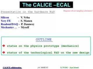
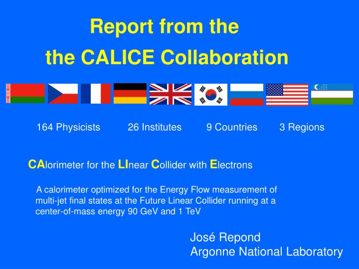
Report from the the CALICE Collaboration. 164 Physicists 26 Institutes 9 Countries 3 Regions. CA lorimeter for the LI near C ollider with E lectrons A calorimeter optimized for the Energy Flow measurement of

E N D
Report from the the CALICE Collaboration 164 Physicists 26 Institutes 9 Countries 3 Regions CAlorimeter for the LInear Collider with Electrons A calorimeter optimized for the Energy Flow measurement of multi-jet final states at the Future Linear Collider running at a center-of-mass energy 90 GeV and 1 TeV José Repond Argonne National Laboratory
Electromagnetic Calorimeter •Silicon – Tungsten France, UK + friends •Silicon – Scintillator ‘LCCAL’ Italy Not part of CALICE Hadronic Calorimeter •Analog readout – ‘Tile HCAL’ Germany, Czech, Russia… •Digital readout – ‘DHCAL’ I Gas Electron Multipliers (GEMs) Texas at Arlington II Resistive Plate Chambers (RPCs) Russia, USA (ANL, Boston, Chicago, FNAL) III Scintillator Northern Illinois IV Short Drift Tubes (SDTs) Protvino Will report on these Others covered by individual talks at this workshop
Structure 2.8 (2×1.4mm of W plates) CALICE ECAL Structure 4.6 (3×1.4mm of W plates) Structure 1.4 (1.4mm of W plates) Metal insert Fine granularity tracking calorimeter Silicon – Tungsten sandwich 1 x 1 cm2 pads 40 layers Simulated energy resolution Prototype for test beams 30 layers Active area 18 x 18 cm2 9720 channels Goal: first tests in 2004 Detector slabs ACTIVE ZONE 10×10 mm2 60 mm Si Wafer with 6×6 pads 60 mm
Front End electronics Shielding PCB Silicon wafer (Cfi / W) structuretype H Detector slab Transverseview Silicon wafer (0.525 mm) PCB (multi-layers) ( 2.4 mm) Al. Shielding 8.5 mm PCB 14 layers Thickness 2.4 mm Composite structure(0.15 mm / layer) Tungsten (1.4 mm, 2×1.4 or 3×1.4 mm)
PCB, Wafers, Chips… PCB board Chips Wafer
Second version being developed…. FLC_PHY1 FLC_PHY2 • Preamp 1 gain (1.5pF) à • Preamp 16 gains (0.2, à Pin - Pin • Low noise (2200e ) - 0.4, 0.8, 1.6pF switchable ) • Shaper Mono gain à • Lower noise (input trans compatibility unipolar improved ) • track & hold Unipolar à • Shaper bigain differential à • track & hold differential à 1 channel MUX out Gain=10 OPA Amp MUX out Gain=1 OPA Front-end electronics: ASIC Measurements on FLC_PHY1 Linearity 0.3% Dynamic range 3.5 pC Noise 2200 e- Pedestal dispersion σ=5mV Satisfactory
Rear-end electronics Developed in the UK Use of CMS Back end
Schedule Mechanical structure Tungsten plates by end of 2003 Assembly in early 2004 FE ASICs FLC_PHY2 tested by September Choice of ASIC Production completed by end of 2003 FE PCB boards Built by February 2004 RE boards Fabrication and assembly in Mar’03 Prototype in beam Cosmic rays first half of 2004 Electrons by mid 2004 Hadrons in 2005
LCCAL Not part of CALICE Collaboration Como, LN Frascati, Padova, Trieste Concept Lead/scintillator plus silicon 45 layers 25 x 25 x 0.3 cm3 Lead 5 x 5 x 0.3 cm3 Scintillator 3 layers of Silicon 1 x 1 cm2 pads at 2, 6, 12 X0
Extensive Tests in Frascati Test Beam Electrons and positrons 50 – 850 MeV Energy selection 1 % Up to 103 electrons/s Energy resolution as expected Npe > 5.1/layer → p.e. statistics negligible Uniformity of light collection at 10 – 20 % level EE E (MeV) Recently inserted Silicon pads
Conclusions and Perspectives LCCAL prototype Almost fully working More Silicon pads are being constructed Third Silicon layer will be fully equipped Test run at Frascati Underway Energy response and resolution as expected Merging Silicon and Energy information: understand multiple hits (>1 e-) Two test beams at Higher Energy in preparation PS and SPS (in 2003) Monte Carlo Simulation Studies of hybrid technique to be initiated
Hadron Calorimeter TESLA TDR HCAL located inside 4T coil Thickness 4.5 λ … Barrel 6.2 λ … Endcap Cell structure Iron 20 mm Active medium 6.5 – 10.0 mm Two options a) Analog hadron calorimeter with scintillator b) Digital hadron calorimeter with …
Analog HCAL Scintillator tiles Area 5 x 5 → 25 x 25 cm2 Thickness 5 mm Longitudinal segmentation 9 … Barrel 12 … Endcap Tests of different plastic scintillator Fiber routing optimization Selection of wavelength-shifting fibers Coupling of WLS-fibres to scintillator Clear fiber selection Connection of WLS and clear fibres Photodetectors Strong R&D program
A few examples… Scintillator PolyVinylToluene based → more expensive BC-408, BC-404… PolyStyrene based → less light SCSN-81, Kuraray, BASF-143… WLS Fiber Routing Stress on fiber → ageing?
Treatment direction WLS Fiber Diameter 1 mm, double clad BC-91A BC-92 Y11(500ppm) … Treatment of fiber end Polishing End reflector Finer sandpaper
42m 20m pixel h Resistor Rn=400 k Al R 50 substrate Ubias 2 mV 2 ns Silicon – Photomultipliers SiPMs R&D at MEPHI (Moscow) together with PULSAR (Russian Industry) Overall size 1.5 x 1.5 mm2 Sensitive area 1 x 1 mm2 Gain 2∙106 at Ubias ~ 50 V Number of pixels 576 → 1000 Recovery time ~100ns
15 photo-electrons 1000 pixels SiPM mounted on tile 4 – 8 photo-electrons 576 pixels Ubias = 53 – 55 V 10 photo-electrons 576 pixels Ubias = 54 V With threshold at ~ 20 photo-electrons Dark rate ~ 2 Hz MIP detection efficiency ~ 97.5%
APDs 3 tiles/APD MA-PMs 3 tiles/pixel SiPMs 1 tile/SiPM Minical Array Stack 27 layers of 9 tiles 5 x 5 x 0.5 cm3 scintillator beam Purpose Cosmic rays starting in August Light Yield Uniformity of response Calibration with MIPs Test of different photo-detectors Long term ageing effects LED monitoring Stability Dynamic range Electron beam Energy resolution Constant term Linearity beam
Outlook Slide by V Korbel shown at Amsterdam Meeting • 1. Enough LY from TFS(~200 photons at photodetector) • 2. APD’s and SI-PMs are the photodetectors which do the task • 3. Preamplifiers with low noise are essential (MIP-noise separation,calibration) • 4. Minical test to establish calibration precision in summer • 5. Now design of prototype boards for APD and Si-PMs (DUBNA) • 6. Photodetectors, large quantity to order in summer: • 1000 APDs or • ~ 5000 Si-PMs or • both types in relevant quantities e.g. ~250/3500 • 7. Prototype stack (1m3) will be build in summer • 8. Assembly of PT-stack with TFS starts in Jan. 2004 • 9. Spring 2004 is used to set up and calibrate all channels with cosmics.
DHCAL: Resistive Plate Chambers - RPCs Only Russian effort (Protvino) for US effort see separate talk Developed RPCs Single gap of 1.2, 1.6 or 2.0 mm 1013Ω∙cm window glass as resistive plates Tests with 16 pads of 1 x 1 cm2 Thickness 4.4 mm (without FEE) Gas mixtures Avalanche mode: TetraFluoroEthane : IB : SF6 = 95 – 98 : 5 : 5 – 2 % Streamer mode : TetraFluoroEthane : IB : Ar/N2 = 80 : 10 : 10 % Tests with Protvino test beam
Tests in avalanche mode To give a few examples… Efficiency and pad multiplicity versus High Voltage Tests with different gases and thresholds Best results for HV = 8.2 kV Threshold = 2.2 mV Efficiency ~ 99% Multiplicity ~ 1.4
Efficiency versus rate for avalanche and streamer mode Maximum rate Streamer mode 4 - 5 Hz/cm2 Avalanche mode ~ 300 Hz/cm2 Pad multiplicity versus charge for different anode thicknesses The thinner the anode the smaller the multiplicity At optimal operating point ~0.5 Hz/cm2 Noise rate versus High Voltage
Comparison of operation modes As an example for 1.2 mm gas gap… Favored
Plans December 2003 Beam tests with 20 layer ‘electromagnetic’ calorimeter 64 pads per layer June 2004 Ready for production and assembly of 1 m3 prototype
DHCAL: Short Drift Tubes - STDs Being developed in Protvino… Efficiency and Multiplicity as function of High Voltage Cell size 1 cm2 x 3 mm GasIB : Ar : TFE = 80 : 10 : 10 Currently using flammable gas exploring performance with other mixtures
DHCAL: Readout schemes Real challenge…. 1 m3 prototype: 400,000 channels!
Readout at Protvino Conceptual design Readout for 64 channels I Conditioning (analog) II FPGA (digital) III Serializer (readout of several FPGA)
COMPARATORS XILINX COOLRUNNER-II CPLD COMPARATORS Readout at Dubna
HCAL: Mechanical Structure of 1 m3 Prototype Structure 40 Layers Each 1 m2 20 mm steel plates Weighs 6 tons! Issues Material of absorber Steel Stainless steel Tolerances on thickness, flatness Active gap Adjustable width Tolerances Support plates, e.g. 2 mm steel Logistics Tests in magnetic field, what B 1 or 2 stacks Who builds it
More information and upcoming meetings… DHCAL meeting in Paris on 28-February-2003 http://polywww.in2p3.fr/flc/agenda_dhcal_280203.html CALICE meeting in Amsterdam on 31-March-2003 http://polywww.in2p3.fr/flc/agenda_CALICE_310303.html ECFA/DESY LC workshop in Amsterdam, April 1 – 4, 2003 http://www.nikhef.nl/ecfa-desy/flashindex.html DHCAL meeting at DESY on June 30, 2003 http://www.hep.anl.gov/repond/DHCAL_Jun_2003_Agenda.ppt A/DHCAL meeting at DESY around October 24, 2003