Download
1 / 40
410 likes | 674 Views
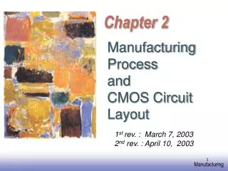
Chapter 2. Manufacturing Process. March 7, 2003. CMOS Process. A Modern CMOS Process. Dual-Well Trench-Isolated CMOS Process. The Manufacturing Process. For a great tour through the IC manufacturing process and its different steps, check

E N D
Chapter 2 ManufacturingProcess March 7, 2003
A Modern CMOS Process Dual-Well Trench-Isolated CMOS Process
The Manufacturing Process For a great tour through the IC manufacturing process and its different steps, check http://www.fullman.com/semiconductors/semiconductors.html
Patterning of SiO2 Chemical or plasma etch Si-substrate Hardened resist SiO 2 (a) Silicon base material Si-substrate Photoresist SiO 2 (d) After development and etching of resist, chemical or plasma etch of SiO 2 Si-substrate Hardened resist (b) After oxidation and deposition SiO of negative photoresist 2 Si-substrate UV-light Patterned (e) After etching optical mask Exposed resist SiO 2 Si-substrate Si-substrate (f) Final result after removal of resist (c) Stepper exposure
Photo-Lithographic Process optical mask oxidation photoresist photoresist coating removal (ashing) stepper exposure Typical operations in a single photolithographic cycle (from [Fullman]). photoresist development acid etch process spin, rinse, dry step
Recurring Process Steps • Diffusion and Ion Implantation: change dopant concentration of some parts of the material. • Deposition: Silicon Nitride Si3N4 (CVD, chemical vapor deposition, Polysilicon (polycrystalline silicon), Aluminum • Etching: Si2O (acid), Plasma etching (dry etching) • Planarization: Chemical-mechanical planarization (CMP) on top of Si2O before deposition of an extra metal layer.
Define active areas Etch and fill trenches Implant well regions Deposit and pattern polysilicon layer Implant source and drain regions and substrate contacts Create contact and via windows Deposit and pattern metal layers CMOS Process at a Glance
p-epi (a) Base material: p+ substrate with p-epi layer + p Si N 3 4 SiO (b) After deposition of gate-oxide and 2 p-epi sacrificial nitride (acts as a buffer layer) + p (c) After plasma etch of insulating trenches using the inverse of the active area mask p + CMOS Process Walk-Through
SiO 2 (d) After trench filling, CMP planarization, and removal of sacrificial nitride n (e) After n-well and V adjust implants Tp p (f) After p-well and V adjust implants Tn CMOS Process Walk-Through
poly(silicon) (g) After polysilicon deposition and etch n + + p (h) After n + source/drain and p + source/drain implants. These steps also dope the polysilicon. SiO 2 (i) After deposition of SiO 2 insulator and contact hole etch. CMOS Process Walk-Through
Al (j) After deposition and patterning of first Al layer. Al SiO 2 (k) After deposition of SiO 2 insulator, etching of via’s, deposition and patterning of second layer of Al. CMOS Process Walk-Through
3D Perspective Polysilicon Aluminum
Layer Color Representation Well (p,n) Yellow Active Area (n+,p+) Green Select (p+,n+) Green Polysilicon Red Metal1 Blue Metal2 Magenta Contact To Poly Black Contact To Diffusion Black Via Black CMOS Process Layers
V DD 3 Out In 1 GND Stick diagram of inverter Sticks Diagram • Dimensionless layout entities • Only topology is important • Final layout generated by “compaction” program
Design Rules • Interface between designer and process engineer • Guidelines for constructing process masks • Unit dimension: Minimum line width • scalable design rules: lambda parameter • absolute dimensions (micron rules)
Intra-Layer Design Rules 4 Metal2 3
Design Rule Checker (on-line check) poly_not_fet to all_diff minimum spacing = 0.14 um.
CMOS Fabrication and Layout • See the supplement data in Web! • http://access.ee.ntu.edu.tw
Packaging Requirements • Electrical: Lowparasitics • Mechanical: Reliable and robust • Thermal: Efficient heat removal • Economical: Cheap • E.g., Ceramic v.s. plastic
Package Types 2 • Bare die • DIP • (dual-in-line package) • PGA (pin-grid-array) • Small-outline IC • Quad flat pack • PLCC • Leadless carrier 7 1 5 4 6 3