Download
1 / 25
310 likes | 598 Views
ESD Protection Design Seminar Jim Sutherland Senior Applications Engineer. Outline. What is ESD? What damage can it cause? Why is the problem growing? What are the issues for the designer? How can we measure it? How can we protect equipment from ESD?. What Is ESD?.

E N D
ESD Protection Design Seminar Jim SutherlandSenior Applications Engineer
Outline • What is ESD? • What damage can it cause? • Why is the problem growing? • What are the issues for the designer? • How can we measure it? • How can we protect equipment from ESD?
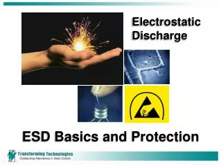
What Is ESD? • ESD = Electro Static Discharge • Generation • Triboelectric (friction causes accumulation of charge) • Induction (field induces charge) • Discharge • Dielectric (air) breakdown • Electric field increases when charged bodies approach each other • Current flow into circuitry
ESD Damage of ICs • Permanent • Oxide breakdown, shorts, opens, latch-up • Temporary • Latch-up, ground bounce • Latent • Degradation from an ESD event
ESD problem is growing • Circuits/Systems • Old - Robust ICs & Low speed signals • New - Sensitive ICs & High speed signals • Environment • Old - Manufacturing / Corporate • New - Home / Outdoors / Person
ESD Issues for the Designer • Must meet ESD specifications • Select ESD tolerant components • Minimize signal degradation (from R,L & C) • Board space / weight / proper design • Component cost • Assembly cost • Lifetime cost (stability) • Test the system
International ESD Standards • Human Body Model (HBM) - for devices • EIA/JESD22-A114-A • ANSI/EOS/ESD-S5.1-1993 • MIL-STD-883 (method 3015) • IEC 1000-4-2:1995 - for systems • Machine Model (MM) - less common • EIA/JESD22-A115-A • ANSI/EOS/ESD-S5.1-1993 • Charge Device Model (CDM) - less common • JESD22-c101
Human Body Model (HBM) • Discharge from 100pF capacitor through 1.5 kOhm resistor • 6 ESD pulses • 3 positive, 3 negative • > 1 sec separation • Pin-to-pin testing • N(N-1)/2 combinations • Used for component characterization • Widely used
HBM Current Waveform Rise Time: 2 nS < Tr <10 nS
IEC 1000-4-2:1995 Standard • Discharge from 150 pF capacitor through 330 ohm resistor • 6 ESD pulses • 3 positive, 3 negative • Used for system characterization • “Contact” v. “Air” discharge • Different levels • Different applications
60ns IEC 1000-4-2 Current Waveform Very fast rise time: Tr < 1nS
IEC 1000-4-2 Test Levels • Contact discharge is the preferred test method - air discharges are not repeatable • Air discharges used where contact discharge cannot be applied • No implied equivalence in test severity between the two test methods
ESD Protection Techniques • Clamp diodes in IC • Not sufficient protection • Shielding • Low effectiveness • Bypass capacitor or series resistor/inductor • Can degrade signal; many components; large board area • Spark gap • Low cost; low stability; large board area • Discrete Zener diodes • High capacitance, many components; large board area • Discrete PN diodes • Low capacitance; many components; large board area • Integrated PN diodes
Integrated Diode Networks • Superior downstream ESD protection • High speed response • ESD current steered to GND or VCC • Minimum Signal Degradation (Low C) • Minimal board space, weight • Low assembly/manufacturing costs • Minimal Design-In Time • Long-term reliability
Choosing an ESD Diode Network • How many lines are needed? • How much capacitance? (e.g. < 5 pF) • What is the HBM rating? (e.g. ±15 kV) • What is the downstream clamp voltage? (e.g. 13 V @ 15 kV HBM pulse) • What is the contact discharge rating? (e.g. ±8 kV) • What is the air discharge rating? (e.g. ±15 kV) • What package? (e.g. 24-pin QSOP)
Vcc Vcc ESD Entry Parasitic L Parasitic L Protected Point Protected Device Device ESD Entry Gnd Point Gnd Poor layout - increased clamp voltage Preferred Layout due to parasitic inductance ESD Diode Network Placement The Need to Keep ESD Diodes Downstream of Line Inductances Also put protection diodes at most likely ESD entry point - the connector
Add Bypass Capacitor • Place Ceramic bypass capacitor (0.1 ~0.2 uF) as close as possible to ESD diode network power rail to shunt ESD current to both power rails • Maybe add Zener in parallel with capacitor to minimize parasitic inductance of bypass capacitor Vcc Protected Device C Gnd
Using a Series Resistor toMinimize Downstream Current • Can be considered for latch-up sensitive applications • Guaranteed clamping voltage limits current downstream (I = V / R) • Only for inputs with high Z • Only for output drivers with low Z • watch out for filtering of signal
Power-down Issues • Diode protected systems that are powered down can drain current from an active high input through the diode to VCC • This can drain batteries and/or damage devices on the same line • To avoid this, isolate VCC from the bypass capacitor with a blocking diode • One diode solution
Component and System Specifications • There is no simple formula to translate system specifications into component specifications • IEC 1000-4-2 Specification is more severe than HBM • Line capacitance and inductance shape the ESD pulse, reducing its peak value • Poor device placement can degrade performance • If there are multiple devices on a line, decide which to protect • The relationship between downstream clamp voltage and downstream protection is not exact
Validating the Design • Define the practical limits of functional failure (e.g. Data integrity, recovery time) • Test only at those places subject to touch during normal operation • Use Contact ES Discharges to coupling planes & conductive surfaces, I/O pins, flex pads, and power pins • Use Air ES Discharges to insulating surfaces, openings at edges of keys, flex cables, vent areas, seams, slots, apertures
Total Solution Cost • ESD failure is a question of statistics • One cannot eliminate all reliability issues • Goal is to minimize total solution cost • Cost of reliability • Cost of protection • Must find proper minimum
Lightning vs. ESD • 200MV 30kA 30us 15kV 45A 80nS