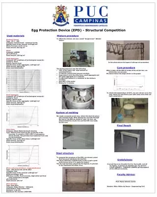
Download
1 / 26
280 likes | 770 Views
ESD Protection In Microwave Device. 2003-21649 이 민 규. Contents. Introduction Material considerations Degradation & Failure MESFET, MODFET, HEMT, HBT Requirements for ESD protection circuits ESD protection circuits & devices Conclusions. Introduction. ESD (Electrostatic Discharge)

E N D
ESD Protection In Microwave Device 2003-21649 이 민 규
Contents • Introduction • Material considerations • Degradation & Failure • MESFET, MODFET, HEMT, HBT • Requirements for ESD protection circuits • ESD protection circuits & devices • Conclusions
Introduction • ESD (Electrostatic Discharge) • 순간적으로 많은 전하가 이동하므로 반도체 소자들에게 큰 손상을 유발 • 대부분 소자의 제작과정이나 패키징 또는 검사과정에서 발생 • 이미 실리콘 반도체에서는 중요한 Reliability aspect • ESD in Microwave Device • 높은 동작 주파수 • 화합물 반도체 • ESD 문제에 더욱 민감한 성질을 지님
Melting point & thermal conductivity of compound semiconductors is lower than of silicon. “Heat up faster and melt earlier” Their susceptibility to ESD is higher as compared to silicon. Material considerations (1)
The melt thresholds for the compound semiconductor devices are about a decade lower than for Si devices. The burn out of compound semiconductors will occur at lower energies. (related to the defect density) Material considerations (2)
Degradation & Failure (1) • The lateral material migration across the GaAs surface -> inter electrode short circuiting bridge • Contact spiking is caused by focused current flow -> filament penetrates junction (short) • Charge injection and oxide degradation and breakdown (related to the defect density)
Degradation & Failure (2) • Filamentation in the semiconductor material -> A current flow in a localized region creates a melt filament (leads to increased leakage current by a resistive path / shorted junction) • Degradation effects related to electromigration in two or three element compound S.C. -> the evaluation of the surface condition is even more complex
Lateral material migration Inter-diffusion between gold-based metal and GaAs-substrate (Ohmic contact) Contact spiking Gate blow-off (Schottky-contact) MESFET Degradation (1)
MESFET Degradation (2) Gate blow-off in MESFET Degradation of ohmic contact
MESFET Degradation (3) Ref. Ragle Dwayne, Ken Decker, and Matthew Loy, “ESD EFFECTS ON GaAs MESFET LIFETIME, IEEE/IRPS, 1993.
The deconfinement of the 2-DEG Formation of a potential barrier These two effects will result in decrease in source-drain current. MODFET Degradation (1) Ref. W.T. Anderson, A. Christou, F.A. Buot, J. Archer, G. Bechtel, H. Cooke, Y.C. Pao, M. Simons, and E.W. Chase, “Reliability of discrete MODFETs : Life testing, Radiation effects, and ESD”, IEEE/IRPS, 1988.
Inter-diffusion of the gold-based ohmic contact metallization with the epitaxial n-GaAs layer affected by hot electrons. WSi2-diffusion barrier and Au top layer -> degradation only at Au contacted the GaAs HEMT Degradation
HBT Degradation (1) ESD current path in a HBT HBT degradation Carbon doped HBT less degradation than Be doped
HBT Degradation (2) Ref. Tim Henderson, “Effects of Electrostatic Discharge on GaAs-Based HBTs”, IEEE, 1997.
Requirements for ESD protection circuits • Have to be integratable with the compound S.C. fabrication process. • Should switch faster than the high frequency devices to be protected. (about a decade faster) • Have to be low-parasitic and to be able to switch high signal levels and very high current densities.
ESD protection circuits & devices • Diodes for ESD Protection • The ESD protection level reached is about 1000V • Applicable frequency range is limited to about 10-15GHz • Multi-finger HBTs, planar doped barrier diodes have very high ESD failure thresholds -> consider as possible ESD protection clamps
Limited in reaction time being in the range of 1ns Based on the physical process of carrier multiplication by ionization of the gas molecules Minimum discharge voltage is about 250V (related to geometry) ESD protection – Gas Discharge
Active electrical device with a vacuum channel parasitic capacitance scale down ( < 0.1pF ) Switching times much lower than 1 ps No power dissipation in the channel Field emitter can handle current densities up to 108A/cm2 ESD protection – Field emission
ESD protection – Diode Protection Ref. F.M. Yamada, A.K. Oki, E.N. Kaneshiro, M.D. Lammert & A.L. Gutierrez-Aitken, “ESD Sensitivity Study of Various Diode Protection Circuits Implemented In A Production 1um GaAs HBT Technology”, EIA, 1999.
Current waveform in various ESD have much lower bandwidth than microwave region Designed the input matching circuit of Ku-band LNA with a high pass filter, which consists of a short stub ESD protection – Using Short-Stub Ref. “Ku-Band Low Noise Amplifier with Using Short-Stub ESD Protection”
ESD protection –Cancellation Circuit Ref. S. Hyvonen, S. Joshi and E. Rosenbaum, “Cancellation technique to provide ESD protection for multi-GHz RF inputs”, ELECTRONIC LETTERS 6th Feb. 2003. Vol. 39
Conclusions • ESD Protection for high frequency compound S.C. based devices and circuits is more critical as compared to silicon. • The frequency range up to 10 GHz • Planar doped barrier diodes, multi-finger HBT are possible ESD protection devices • The frequency range over 10 GHz • Field emission diode and triode are possible ESD protection devices.
References (1) • K. Bock, “ESD issues in compound semiconductor high-frequency devices and circuits”, Microelectronics Reliability 38, 1998:1781-1793. • K. Bock, “Properties of GaAs Field Emitter Array Structures for ESD-Protection of MMIC”. • F.M. Yamada, A.K. Oki, E.N. Kaneshiro, M.D. Lammert & A.L. Gutierrez-Aitken, “ESD Sensitivity Study of Various Diode Protection Circuits Implemented In A Production 1um GaAs HBT Technology”, EIA, 1999. • Chang-Kun Park, Min-Gun Kim, Chung-Han Kim, and Songcheol Hong, “Ku-Band Low Noise Amplifier with Using Short-Stub ESD Protection”, IEEE Radio Frequency Integrated Circuits Symposium, 2003. • Charles Y. Chu, and G.P. Li, “ESD Performance Optimization of Ballast Resistor On Power AlGaAs/GaAs Heterojunction Bipolar Transistor Technology”, EOS/ESD Symposium, 1999:235. • S. Hyvonen, S. Joshi and E. Rosenbaum, “Cancellation technique to provide ESD protection for multi-GHz RF inputs”, Electronics Letters 6th Feb. 2003: Vol.39 No.3.
References (2) • Dwayne Ragle, Ken Decker, and Matthew Loy, “ESD Effects on GaAs MESFET Lifetime”, IEEE/IRPS, 1993. • W.T. Anderson, A. Christou, F.A. Buot, J. Archer, G. Bechtel, H. Cooke, Y.C. Pao, M. Simons, and E.W. Chase, “Reliability of Discrete MODFETs: Life Testing, Radiation Effect, And ESD”, IEEE/IRPS, 1988. • Tim Henderson, “Effects of Electrostatic Discharge on GaAs-Based HBTs”, IEEE, 1997.