Download
1 / 36
360 likes | 514 Views
Physical Principles of Nanoelectromechanical Devices. Robert Shekhter. University of Gothenburg, Sweden. Lecture 1 : Introduction to nanoelectromechanical systems (NEMS). 2 /35. Electromechanics and Charge Metrology.

E N D
PhysicalPrinciples of NanoelectromechanicalDevices Robert Shekhter University of Gothenburg, Sweden
Lecture 1: Introduction to nanoelectromechanical systems (NEMS) 2/35 Electromechanics and Charge Metrology Theelectroscopewasanearlyscientificinstrumentusedtodetectthepresenceandmagnitudeofelectricchargeon a body. WilliamGilbert BornonMay 24, 1544, inColchester, England DiedonDec. 10, 1603, inLondon
Lecture 1: Introduction to nanoelectromechanical systems (NEMS) 3/35 Downsizing of Electro-Mechanical Devices MacroscopicElectromechanicalDevice Micro-ElectromechanicalAccelerometer (AirbagSensor) A smallintegratedcircuitwithintegratedmicromechanicalelements, whichmoveinresponsetorapiddeceleration. Thismotioncauses a changeincapacitance, whichisdetectedbytheelectronicsonthechipthatthensendsasignaltofiretheairbag. Nano-ElectromechanicalMachineryintheLivingCell Ionchannelsmakeitpossibleforcellstogenerateandtransmitelectricalsignals, andarethebasicmolecularbuildingblocksinthenervoussystem. Rapidtransport, ionselectivity, andelectricallycontrolledchannelgatingarecentraltotheirfunctionality.
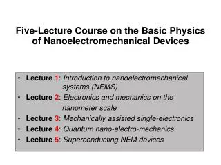
Five-Lecture Course on the Basic Physics of Nanoelectromechanical Devices • Lecture 1: Introduction to nanoelectromechanical systems (NEMS) • Lecture 2: Electronics and mechanics on the • nanometer scale • Lecture 3: Mechanically assisted single-electronics • Lecture 4: Quantum nano-electro-mechanics • Lecture 5: Superconducting NEM devices
References Book: Andrew N. Cleland, Foundation of Nanomechanics Springer,2003 (Chapter7,esp.7.1.4, Chapter 8,9); Reviews: R.Shekhter et al. Low.Tepmp.Phys. 35, 662 (2009); J.Phys. Cond.Mat. 15, R 441 (2003) J. Comp.Theor.Nanosc., 4, 860 (2007)
Lecture 1: Introduction to nanoelectromechanical systems (NEMS) Outline • WhyNEMS? • Fabricationmethods • Actuationanddetectionmethods
Lecture 1: Introduction to nanoelectromechanical systems (NEMS) 7/35 Part 1Why NEMS?
Lecture 1: Introduction to nanoelectromechanical systems (NEMS) 8/35 MEMS – already a mature technology MEMS applications can be found in the information technology, transport industry, medicine and many other fields totalling more than1000 million dollars of revenues per year.
Lecture 1: Introduction to nanoelectromechanical systems (NEMS) 9/35 Device applications… • Smaller, cheaper, faster, lower power • consumption • ”Phones of the future”. NEM-devices are • in the right frequency range (1-5 GHz) to • replace elements in cell phones • Better frequency selectivity (higher Q), • lower power consumption • New sensor applications • Needed: High Q, high frequency … andinteresting “cuttingedge” physics.
Lecture 1: Introduction to nanoelectromechanical systems (NEMS) 10/35 New Functionality and Possible Applications of Nanoscale Electromechanics • NEM sensing (sensing of mass, displacements and forces on an atomic scale) • Mechanical control and mechanicallyassistedtransportation of single electrons • Mechanically controllable quantum point contacts
Lecture 1: Introduction to nanoelectromechanical systems (NEMS) 11/35 Resonant Mass Sensors (mass sensing on the level of single molecules) dMmin≈ M/Q low M , high w0 , high Q See review in Nature Nanotech. 4, 445 (2009) [Roukes’ group (Caltech)] Sensitivity: ~200 Da Nature Nanotech. 3, 533 (2008); Nano Lett. 8, 4342 (2008) Roukes’ group (Caltech): Nature Nanotechn 4, 445 2009 (Roukes) Sensitivity: 100 zepto-grams K.L.Ekincietal. APL 64, 4469 (2004) 200 Dalton=3.6 10-22g
Lecture 1: Introduction to nanoelectromechanical systems (NEMS) 12/35 Biomolecular Recognition Surface stress changes the nanomechanical response of cantilevers.Bending of cantilevers detected by an optical deflection technique. J. Fritzetal., Science 288, 316 (2000)
Lecture 1: Introduction to nanoelectromechanical systems (NEMS) 13/35 MEMS/NEMS Devices as Electrometers NEMS analogueofCoulomb’s torsionalelectrometerfrom 1784. A chargeonthegateaffectsthe resonancefrequency. • measured sensitivity (300 K): 0.1eHz-1/2 • ultimate sens. (300 K): 2 10-5 eHz-1/2 A.N. Cleland and M.L. Roukes, Nature 392, 160 (1998)
Lecture 1: Introduction to nanoelectromechanical systems (NEMS) 14/35 Detection of Nanomechanical Displacements Blurringin STM fromthermal vibrations, NanoLett. 3, 1577 (2003) (Schönenberger, Basel) Tuningbandgapwithstrain PRL 90, 156401 (McEuen)
Lecture 1: Introduction to nanoelectromechanical systems (NEMS) 15/35 Nanomechanical Manipulation (Nanotweezer) Left: A nanotweezer made of two isolated CNTs is opened and closed by applying a bias voltage. Top: Optical micrographs showing the sequential process of nano-tweezer manipulation of polystyrene nanoclusters containing fluorescent dye molecules. P. Kim and C.M. Lieber, Science 286, 2148 (1999)
Lecture 1: Introduction to nanoelectromechanical systems (NEMS) 16/35 Nanomechanical Single-Electron Transistor biasvolatge gate voltage Nature 407, 57 (2000) (P.L. McEuen, Cornell)
Lecture 1: Introduction to nanoelectromechanical systems (NEMS) 17/35 Mechanical “Sharpening” of Quantum Point Contact Top left: Top and side view of a mechanically controlled break junction, with notched wire (1), two fixed counter supports (2), bending beam (3), drops of epoxy adhesive (4) and stacked piezo element (5). Top right: Electron microscopy image of a gold break junction on SiO2 cantilvers Right: Sharpening of the contact by mechanical elongation N. Agrait et al., Phys. Rep. 377, 81 (2003)
Lecture 1: Introduction to nanoelectromechanical systems (NEMS) 18/35 Nanoelectromechanics of the Breaking of an Atomic Gold Wire
Lecture 1: Introduction to nanoelectromechanical systems (NEMS) 19/35 Part 2Fabricationmethods
Lecture 1: Introduction to nanoelectromechanical systems (NEMS) 20/35 Top-Down – Semiconducting Suspended Nanowires
Lecture 1: Introduction to nanoelectromechanical systems (NEMS) 21/35 Bottom-Up – Self-Assembled Metal-Organic Composites Molecular manufacturing – a way to designmaterials on the nanometer scale. Encapsulated 4 nm Au particles self-assembled into a 2D array supported by a thin film, Anders et al., 1995 Scheme for molecular manufacturing
Lecture 1: Introduction to nanoelectromechanical systems (NEMS) 22/35 Molecular Junctions Methods to fabricatemolecularjunctions
Basic Characteristics Self-Assembled Materials Electrical – heteroconducting Mechanical - heteroelastic Quantumcoherence Coulombcorrelations Electromechanical coupling Lecture 1: Introduction to nanoelectromechanical systems (NEMS) 23/35 Materialsproperties Electronicproperties
Lecture 1: Introduction to nanoelectromechanical systems (NEMS) 24/35 Suspended CNTs
Lecture 1: Introduction to nanoelectromechanical systems (NEMS) 25/35 Suspended CNTs
Lecture 1: Introduction to nanoelectromechanical systems (NEMS) 26/35 Part 3Actuationanddetectionmethods
Methods of Actuation and Detection Lecture 1: Introduction to nanoelectromechanical systems (NEMS) 27/35 STM detection Capacitive actuation and detection Magnetomotivemethod Tunnel spectroscopy and point-contact spectroscopy of NEM vibrations Mechanically assisted transport of electrons
Lecture 1: Introduction to nanoelectromechanical systems (NEMS) 28/35 Different Types of NEM Coupling C(x) • Capacitive coupling • Tunneling coupling • Shuttle coupling • Inductive coupling R(x) C(x) R(x) I Lorentz force for given I FL H . Electromotive force at I = 0 for given v E v
Lecture 1: Introduction to nanoelectromechanical systems (NEMS) 29/35 Electrostatic Actuation and Detection Au/Crelectrodes (Au/Cr) areshowninyellow, andthesiliconoxidesurfaceingrey. Thesidesofthetrench, typically1.2–1.5 µmwideand500 nmdeep, aremarkedwithdashedlines. A suspendednanotubecanbeseenbridgingthetrench. 300 nm Non-zero only if beam moves V. Sazonovaetal., Nature431, 284 (2004)
Lecture 1: Introduction to nanoelectromechanical systems (NEMS) 30/35 Intrinsic Thermal Vibrations of Single-Wall Carbon Nanotubes Imaged by a Scanning Electron Microscope (SEM) Babicetal., NanoLetters 3, 1577 (2003)
Lecture 1: Introduction to nanoelectromechanical systems (NEMS) 31/35 Magnetomotive Actuation and Detection
Lecture 1: Introduction to nanoelectromechanical systems (NEMS) 32/35 Magnetomotive Method: Pt Nanowire
Lecture 1: Introduction to nanoelectromechanical systems (NEMS) 33/35 Magnetomotive Method: Breaking the GHz Barrier
Lecture 1: Introduction to nanoelectromechanical systems (NEMS) 34/35 Measuring Eigenfrequencies: Phonon Assisted Tunneling
Lecture 1: Introduction to nanoelectromechanical systems (NEMS) 35/35 Point Contact Spectroscopy in a H2 Molecule
Lecture 1: Introduction to nanoelectromechanical systems (NEMS) 36/35 Vibration Modes for Deuterium, Pt-D2-Pt