Download
1 / 54
960 likes | 1.66k Views
SIGNAL CONDITIONING. By: Nor Farhani Zakaria School of Microelectronic Eng. OBJECTIVES. Explain the purpose of analog signal conditioning . Design a Whe atstone bridge circuit to convert resistance change to voltage change .

E N D
SIGNAL CONDITIONING By: Nor FarhaniZakaria School of Microelectronic Eng.
OBJECTIVES • Explain the purpose of analog signalconditioning. • Design a Wheatstone bridge circuit to convert resistance change to voltagechange. • Design RC low-pass and high pass filter circuits to eliminate unwantedsignals. • Understanding the schematics of four common op amp circuits and provide the transferfunctions. • Explain the operation of an instrumentation amplifier and draw itsschematic. • Design an analog signal-conditioning system to convert an input range of voltages to some de sired output range ofvoltage. • Design analog signal conditioning so that some rangeof resistance variations is converted into a de sired range of voltage variation.
Sensors produce different kind ofsignals • Voltage output or Currentoutput • Can’t necessarily take sensor output and put right into Microprocessor ADC or logicinput • Signal mayneed: • High to low impedance buffer, current to voltage conversion, gain, de tection, & filtering.
Signal Conditioning: • Convert signal to a form suitable for interface with other elements • Signal from detector stage has to be modified (conditioned) in order to make it more usable. • This signals is then to be use in later stage of system that may consist of indicating, recording and processing elements. • for passive transducers : excitation from external power source & amplification. • for active transducer : amplification (produced higher level voltage)
Electronic Aided Conditioning 1 3 Numbers 2 Characteristic of Electrical Signal Convert signal to a form suitable for interface with other elements
DC Signal Conditioning Usually used for common resistance transducers (e.g. potentiometers & strain gauge) Eliminate noise & HF output e.g.strain gauge Disadvantage : Low drift (Change in the value of the parameter without any external change Or change in output even though the input was provided.)
AC Signal Conditioning Usually used for variable reactance transducers & system in which signals have to be transmitted via long cables. OUTPUT: Amplitude modulated carrier demodulator e.g. variable resistance/inductance type 50kHz-200kHz (5-10 times of signal freq.) Disadvantage: difficult to have stable carrier oscillator prevention by active filters
The Principles Convert signal to a form suitable for interface with otherelements Signal level and bias changes LinearizationConversion Filteringand impedancematching Concept ofloading SignalConditioning Wednesday, March 27,13
Signal Level and biaschanges adjusting the level (magnitude) and bias (zero value) of some voltage representing a processvariable amplification vs attenuation --> usesamplifier Linearization The purpose of linearization is to provide an output that varies linearly with some variable even if the sensor output doesnot. Wednesday, March 27,13
Conversion Convert one type of electrical variation intoanother. Signal Transmission (Voltage to current, Current to Voltageconverter) Digital Interface (ADC requires 0-5Vinput) Filtering & impedancematching Filtering-Eliminate unwanted signals in the process-controlloop Impedance matching-transducer internal impedance or line impedance can cause error in me asurement of a dynamicvariable. Wednesday, March 27,13
Concept ofloading Concern -loading of one circuit byanother. Thévenin's theorem for linear electrical net works states thatany combination of voltage source s, current source s, and resistors with t wo terminals is electrically equivalent to a single voltage source Vth and a single series resistor Rth. this equivalent voltage Vth is voltage obtained at theterminalsA-B of thenetwork with terminal A-B opencircuits this equivalent resistance Rth is the resistance obtained at terminal A-B of the net work with all its current source open circuited and all voltage sources short circuited Wednesday, March 27,13
Example of Signal Conditioning • Passive Circuits • DividerCircuits • Bridge Circuits • RC Filters • Operational amplifier (OP-AMP)
DividerCircuits The simple voltage divider can often be used to convertresistance variation into voltagevariation. Rtotal=R1+R2 VsVs I = = total R R1+ R2 total R2 VD = ItotalR2 = Vs R1 +R2 either R1orR2 can be yoursensor
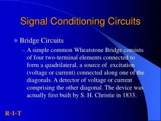
BridgeCircuits used to convert impedance variations into voltagevariations operate in the unbalance operation when the ratio areequal where R1R4=R2R3, voltage across a & b will bezero any change on the resistance value which cause the bridge unbalance, will producea voltage across the a & b point.
BridgeCircuits Vt h = Va–Vb Va= potential of point a Vb = potential of point b -
BridgeCircuits When a galvanome ter is used for a null de tector, it is convenient to use the Thévenin equivalent circuit of the bridge. Thevenin equivalent resistance R1R3R2R4 Rth = + R1+R3R2+R4 Vth IG= R +R th G Wednesday, March 27,13
BridgeCircuits LEADCOMPENSATION When bridge circuit may be located at considerable distance from the sensor whose resistance changes are to be measured. any changes in lead resistance are introduced equally into both arms of the bridge circuit, thuscausing no effective change in bridge offset For remote sensor applications, this compensation system is used to avoid errors from leadresistance Wire 3, is the power lead and has no influence on the bridgebalance If wire 2 changes inresistance--> change R4. Wire 1 changes by the same amount (& exposed to the same environment) --> changeR3
BridgeCircuits Bridge off-null voltage is clearly nonlinear for large-scale changes inresistance. • Primary applicationof bridgecircuitsis to convert variations of resistance into variations of voltage • If the range of resistance variation is small and centered about the null value, Then the nonlinearity of voltage resistance is small. However, for small ranges of resistance change, the off-null voltage is nearlylinear. Wednesday, March 27,13
Amplification Required in the system to improve the signal strength which is typically in the low level range of less than a fewmV. In some case s, amplifiers is necessary in providing impedance matchingand isolation. One of the very known important amplifier is the operational amplifiers (OP-AMP)
Operational Amplifier("op-amp") An operational amplifier ("op-amp") is a DC-coupled high-gain electronic voltage amplifier with a differential input and, usually, a single-endedoutput. An op-amp produces an output voltage that is typically hundreds of thousands time s larger than the voltage difference bet ween its inputterminals. Can be used to performs an important functions for signal conditioningand processing like isolation, addition, inversion, multiplication, subtraction anddivision. Other mathematical operations can be also perform such as integrationand differentiation.
The “Ideal” OpAmpModel Circuit for an ide al OpAmp (operationalamplifier.) The voltage gain is infinite – Avo = ∞. The input resistance is infinite – rin = ∞. The output resistance is zero – ro = 0. The bandwidth is infinite – BW = ∞. There is zero input offset voltage – Eo = 0 if Ein = 0.
Negative FeedbackOpAmp Transimpedance Amplifier Non-Inverting Amplifier VoltageFollower InvertingAmplifier InvertingSummer Tuesday, April 2,13
TransimpedenceAmplifier IF Zin mean Vout IFR Iin Vout F IinRF Converts a current into avoltage Generates a proportional (w. Rf) voltage from an input current Produce s a low-impedance output that can drivea microcomputer’s A-D converter, forexample Tuesday, April 2,13
Non-Inverting Op-Amp Gain can be adjusted from unity upward via resistor ratio No voltage difference between inputs Resistors act like voltage divider
VoltageFollower Act as a buffer – isolates circuit from the output (driver). Has a high input impedance and low output impedance. Av = 1 A unity-gain buffer to enable high-impedance sources to drive low-impedanceloads Tuesday, April 2,13
APPLICATION: Voltage Follower
Inverting Op-Amp Inverts signal, voltage gain varies from zero upward with the ratio of two resistors Gain (Av) Two important rules to remember: 1. No Current Flows into the Input Terminals 2. The Differential Input Voltage is Zero as V1 = V2 = 0 (Virtual Ground)
APPLICATION: • Summing Op-Amp • inverting amplifier accept two or more inputs and produce a weighted sum. • op-amp adjusts itself to draw total input current iin through Rf (iin = if) Analysis:
APPLICATION of summing op AMP: DAC – DIGITAL ANALOG CONVERTER • 4-Bit BINARY Weighted-Resistor DAC • “Weighted Resistors” based on bit • Reduces current by a factor of 2 for each bit MSB R 2R 4R 8R
Op-Amp Difference Amplifier • produces an output proportional to the difference between the two inputs • op-amp subtracts the inputs and amplifies their difference. NON -IDEAL CASE: Analysis: IDEAL CASE:
Comparator Makesananalogsignalintoa1-bitdigitalsignal(ADC) Directly drives logic pin onmicroprocessor Detects when signal is abovethreshold A fixed reference voltage Vref is applied to the inverting (-) input terminal and sinusoidal signal Vin is applied to the non-inverting (+) input terminal. When vin e xceeds Vref the output voltage goes to positive saturation because the voltage at the (-) input is smaller than at the (+) input. On the other hand, when vin is less than Vref the output voltage goes to negative saturation. Thus output voltage uout changes from one saturation level to another whenever vin = Vref Tuesday, April 2,13
SchmidtTrigger Deadband Suppresses jitter and spurious triggering from noisysignals Deadband thresholds, V+ and V-, can be calculated viasuperposition Ground VIN-, and with R1 and R2 as a voltage divider on Vout , calculate the voltage at the OpAmp’s non-invertingpin Note that this assumes a low-impedance VIN (source impedance sums withR1) Tuesday, April 2,13
The Basic InstrumentationAmplifier Buffer each leg of the differential amplifier by a voltage follower Impedance is now extremely high at bothinputs Impedance can be set by a shunt resistor across inputs This is a balanced “instrumentation”amplifier Tuesday, April 2,13
The Three-OpAmp InstrumentationAmplifier Gain is varied by changing only one resistor, R1 No need to re-trim other components for a gain change Gain at first stages is better forsignal/noise This is the instrumentation amplifier ofchoice Tuesday, April 2,13
An Instrumentation Amplifier with TwoOpAmps Can use when you only have space for a dual OpAmp Gain change requires two resistors to be adjusted Common mode sensitivity increases athigher frequency Tuesday, April 2,13
RCFilters • To eliminate unwanted noise signals from me asurements, it is often necessary touse circuits that block certain frequencies orbands of frequencies. Wednesday, March 27,13
RCFilters DesignGuideline findthecriticalfrequencythatwillsatisfythedesign criteria Wednesday, March 27,13
Types of filters (a) Low pass (b) High pass (c) Band pass (d) Band stop (e) All pass
Basic Low Pass Filter (LPF) • low frequencies : capacitive reactance is very high • capacitor circuit acts like an open circuit. Vo = Vi with Av=1. • very high frequencies: capacitive reactance is very low • Vo << Vi. Av drops off gradually with increasing f Low frequencies are passed, high frequencies are attenuated. Wednesday, March 27,13
Basic Low Pass Filter Example: • A solid barrier acts as a low-pass filter for sound waves. When music is playing in another room, the low notes are easily heard, while the high notes are largely filtered out. • very loud music played in one car is heard as a low throbbing by occupants of other cars, because the closed vehicles(and air gap) function as a very low-pass filter. • Radio transmitters use low-pass filters to block harmonic emissions which might cause interference with other communication.
Low Pass Filter LPF in Time domain: converts a square wave “step” response input signal into a triangular shaped waveform output as the capacitor charges and discharges. A Triangular waveform consists of alternate but equal, positive and negative ramps.
Active Filters • Generally the impedances are used in the inverting amplifiers using operational amplifiers. • Advantages of Active Filter over Passive Filter: • Gain and frequency adjustment flexibility • Since the OpAmp is capable of providing a gain, the input signal is not attenuated, as in a passive filter. Active filter is easy to tune. • No loading problem • Because of the high input resistance and low output resistant of the OpAmp, the active filter does not cause loading of the source or load. • Cost • Active filter more economical than passive filter because of the variety of cheaper OpAmps available and the absence of inductors.
Application: LPF in Butterworth filter V1 First order butterworth filter V2 where V1
Basic High Pass Filter • low frequencies: Vo<< Vi, gain is small • High frequencies: gain approaches unity. High frequencies are passed, low frequencies are attenuated. Wednesday, March 27,13
Band Pass Filter • Can be constructed by cascading LPF and HPF. • At frequencies below the pass band, BPF behave like HPF while above the pass band frequencies the BPF acts like LPF. • In pass band, the BPF circuit is almost as a resistive network. Only frequencies in frequencies band are attenuated.
Band Pass Filter • defined as a wide band pass if its figure of merit or quality factor Q < 10. • Q = measure of selectivity higher Q means more selective the filter is =narrower band width • If Q > 10, the filter is a narrow Band Pass
Band Reject (Stop) Filter • Twin T-network • At very low and high frequencies the gain is almost unity • between the two there is a frequency where the gain become zero, fo. • fo= Notch Frequency. Tuesday, April 2,13