Download
1 / 21
210 likes | 339 Views
Graphene Nanoelectronics: Making Tomorrow’s Computers from a Pencil Trace. San -Lab converts thoughts into shape…. A SHORT INTRO OF San -Lab.

E N D
Graphene Nanoelectronics: Making Tomorrow’s Computers from a Pencil Trace San-Lab converts thoughts into shape…..
A SHORT INTRO OFSan-Lab • SantechInternational Inc, USA,San-Labis a Research and Development service based Organization dedicated to the emerging fields of next generation Nano-electronics & Telecommunication specializing in innovation in convergence connectivity. • San-Labhas taken strategic decision to have Partnership with the College of Nanoscale Science and Engineering (CNSE) of different reputed Universities of USA and IIT/IIS of India. • San-Labhas arranged to have IBM high-performance servers to its 300mm wafer nano-electronics research facilities. • Santechhas also initiated to open up under the name ofSan-Labin “Santech Research Valley” back in Kolkata, India, under Indian Government’s designated Special Economic Zone.. • San-Labwill provide Research at least cost with World Class benefits of R&D.
MISSION OFSan-Lab • The primary objective ofSan-Labis to focus in R&D in the field of Nano-electronics, Telecommunications and Emerging Science. • To enable research in the above areas on next generation in collaboration with USA Universities and Indian Government Institutions (Indian Institute of Technology and Indian Institute of Science). • To work shoulder to shoulder with the World’s reputed Universities and with their researchers including EDC (Incubators).
San-LabCHIEF ARCHITECT’S PROFILE • San-Labis the brain child of Dr. Santosh Mukherjee, Architect and President of Santech International Inc,San-Lab. • Dr. Mukherjee is an young, award wining, energetic and emerging technologist & Scientist, who is one of the pioneer in the Technology fields of Telecommunication and Nano-electronics. • He has 24yrs of professional experiences with foreign blue chip companies and also having experience to work as academia with the best Universities of USA. • Dr Mukherjee has finished his D.Sc and PhD from USA in the relevant field of interest. • He has 2 patents approved by USPGOV and 6 are in the process. He has published many similar kinds of technological books & journals. • Dr Mukherjee is also associated with AMA, ADB, States Technological Council of USA, Universities of USA Incubation Centers, Asian Development Bank, Member of Indian Government Tech Diaspora. • Recipients of the award, “Best Technologist & Emerging Scientist of the Yr 2003” from World Business Forum, in the Capitol Hill, Washington, USA.
San-LabUSA & INDIA • San-Labis an emerging Technological Research and Development organization having presence in India, Kolkata as “San-Tech Research Valley”. It has its main centre in in USA as Santech International Inc, San-Lab USA. • TheSan-Labhas Partnered with: (a) US Universities/ Incubators/ EDC (Enterprise Development Centre). (b) Federal and State Government Research Institutes. (c) It will revolutionize the World R & D scenario as well as concept ofSan-Labby providing Orientation Program in the above areas. (d) Indian Institute of Technology /Indian Institute Science, Government of India. (e) Indian Government Research Institutes.
USA UNIVERSITY(College of Nanoscale Engineering) • San-Labhas strategically determined to partner with Universities of USA, Canada, Singapore & India who are pioneers in the areas of Nano- electronics, Telecommunications and Emerging Science. • Some of the USA Universities are, for example, Stanford University, Perdue University, Albany University, Waterloo University and many others. • San-Labis working in compliance with States Science & Technical Commissions as well as Technological Councils of USA.
SAN-LAB -IIT RESEARCH INITIATIVE • IIT (Indian Institute of Technology) have shaken hands with San-Labfor the Convergence as it is a government of India pioneer. Institute of India has partnered with San-Lab to conduct R&D activities in Telecom areas. • San-Lab – IIT Research Initiative is a joint venture program to include research work in various Telecom Convergence of switch. • San-Lab Research Initiative also to undergo wireless based device drivers. • San-Lab IIT Research Initiative is also to undergo wireless based device drivers. • So, the Indian Institute of Technology is working upon the Convergence Switch which removes the barriers to the cost-effective convergence of voice and data.
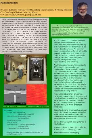
San-LabR&D INITIATIVE San-LabNano-Electronics R&D • TheSan-Lab has taken strategic decision to have Partnership with the College of Nanoscale Science and Engineering (CNSE) of different reputed University of USA & Indian Institute of Science, Haldia (Government of India). • San-Lab has arranged to have IBM high-performance servers to its 300mm wafer nano-electronics research facilities, enabling its next-generation nanotechnology research and development and distributed workforce development and training initiatives. • San-Lab is building a computing infrastructure designed to collect, store, analyze and disseminate large amounts of nanotechnology research data required for further developments. • San-Lab Nano-electronics expects the benefits of the technology to include supporting the development and commercialization of advanced high tech products. These products include faster optical and optoelectronic interconnects for high-speed telecommunications; real-time three-dimensional imaging; biochips for DNA sequencing and blood testing; advanced nano-sensors for energy and environmental applications, and portable, lighter, and more efficient electronic devices for high-resolution display applications.
San-Lab R&D INITIATIVE San-LabTelecom R&D • Apart from doing research on convergence switch, the other current areas of research focus include- • Routing and path computation in optical networks, optimal resource allocation in wireless networks, and high performance computer networks and applications. • Activities in the broad area of communication networks and systems, with emphasis on, architecture, modeling, performance analysis, multi-access, mobility and call control, switching, telegraphic and protocols. • The areas of interest include but are not limited to broadband communications, high performance computer networks. • Wireless based mission critical applications including Mobile Computing and mobile communications, and digital video and multimedia communications. • The primary objective of this laboratory is to foster cooperative research programs with academia and research agencies at the national and international level.
R&D OUTSOURCING ACTIVITIES & BENEFITS • Providing R & D support services to Telecom/Nanotech and emerging technological company. • Providing consulting services to these companies to identify and segregate the components of R&D to be outsourced and to provide proper services to the R&D Organizations to make them understand about the R&D assignments. • To Develop a dynamic website portal to use it as transparent media to broadcast the progress of the given R&D assignments to San-Lab. It will encompass the entire details from the task distributions, team monitoring and also re-join the developed assignments with the main source of the product. • Helping customer's R&D dept to provide related valued consulting expertise from San-Lab experts from USA and India in the areas exploring their ideas, ultimately to help to reach to its viable product solution. Both the team will work in sync to reach to a common goal, to accomplish ultimate error free, economical, practical, market oriented and mission critical solution. • The activities also include to provide a clear concept of the product from the inception to the completion also to help to develop Worldwide market strategy report before actual launch of the same product. • Provide positive due diligence in terms of product development & marketing, they will make use of market information of USA, UK, Canada, Singapore and India so that the ultimate products are based on the World Standard Platform.
Marketing Benefits • San-Labhelps the companies to develop model products companies can make model products before actual launch in the market within a definite time. • As part of product development and marketing due diligence they can make use of USA, UK and India and neighboring countries market as a platform to standardize their product. • San-Lab will help these companies emphasize on Marketing in Singapore, India and South Asia where forecasted market is of $1000 billions. Market Perspective • We are projecting that nanoelectronics will be ranked at 1,000 or 200 times the transistor technology, 100 times the IC technology and 50 times the Internet technology. • The first generation includes nanoelectronics products being sold for the next ten years, to 2014. • The second generation of nanoelectronics includes molecular electronics, self-assembly using biotechnology, and quantum computing.
San-Lab India INFRASTRUCTURERESEARCH & DEVELOPMENTIT & ITES San-Labwill perform mainly catering following activities: • San-LabR&D initiatives • R& D Global Initiatives • R&D Consulting • R&D Training and Orientation • San-Lab and University joint partnering initiative
San-LabR&D GLOBAL FACILITIES (INDIA & USA) • San-Lab will impliment a new formulation new simulation techniques, developing a new generation of software tools, and bringing this new understanding and perspective into the research lab. • San-Labaddress problems in atomistic phenomena, quantum transport, percolative transport in inhomogeneous media, reliability, and the connection of nanoelectronics to new problems such as biology, medicine and energy. • San-Labwork closely with experimentalists to understand nanoscale phenomena and to explore new device concepts. • San-Lab in the course of this work, will produce open source software tools and educational resources that we sharewith the community through the San-Hub. • San-Lab is building a computing infrastructure designed to collect, store, analyze and disseminate large amounts of nanotechnology researchdata. • San-Lab University Partnership to provide University faculty, students, and university an impressive and exciting array of state-of-the-art capabilities that greatly enhance our educational and research opportunities in our Nano-electronics interest areas.
San-Labintends to use the IBM hardware to facilitate important research into the next-generation 56-nanometer (nm) integrated circuit (IC) technology node and beyond having complex and challenging technology transitions • San-Laband University partnering initiative towards research and development investment to enable next-generation chip-making technologies reducing time and cost perspective. • San-Lab partnership with the College of Nanoscale Science and Engineering at the University is reducing research and development costs, speeding innovation and positioning San-Lab, New Jersey center will become the epicenter of an impending major shift in the semiconductor industry • San-LabNano Technology expects the benefits of the technology to include supporting the development and commercialization of advanced high tech products for the information superhighway. • (a) To include faster optical and optoelectronic interconnects for high-speed telecommunications. • (b) Real-time three-dimensional imaging; biochips for DNA sequencing and blood testing. • (c) Advanced nano-sensors for energy and environmental applications. • (d) Portable, lighter and more efficient electronic devices for high-resolution display applications in the various practical use. • TheSan-LabResearchers atSan-Lab facilities also will use the IBM servers which will support the IBM servers will support - • (a) sophisticated and robust IT infrastructure • (b) Designed to deliver advanced functionality. • (c) Automated tool operation and data collection, secure data management. • (d) Precise 300mm wafer tracking and control, and more.
SAN-LABIT & ITES ACTIVITIES • IT Services include : SANTOS Products • E-Solutions • System Integration SANTOS Talkable office System • Application Development Comprising of Legal Setup • Remote NOC Medical Setup & • Remote Database Standard Setup • ITE Services include: • Web Maintenance and support SANTOS EMS(SANTOS Enterprise Management Solution) • Support Services Consisting of Modules: • KPO HR Management • BPO Payroll System • Web Design and Hosting Inventory System • 3D Animations Sales & Marketing System • Learning Modules for web and in CDROM CRM System • Print and Publication Support • Data Entry Operations
R&D TEST BEDS WIRELES COMMUNICATIONS • San-Labhas decided soon to create the Distributed Broadband Wireless Test Bed at the San-Lab Communications Research Centre (CRC) USA, Singapore and India. The work is a collaboration of the various reputed Research Institute's and founding industry partners. • The new test-bed will be established in collaboration with USA Universities and State Science and Technology Commission as a distributed laboratory through dedicated scientific web portal. • San-Labwill be capable to conduct remote Research and Development on wireless transmission of voice, video and data communications and their connections with broadband networks. The facility will be available for the USA ,Canada, Latin America an industry to test and demonstrate products and services in the emerging field of broadband wireless communications systems as well as mobile computing. • San-Labintents to have a national network of three specialized Wireless/Mobile Test Bed Projects operated by independent corporations that are available to U.S. and international corporations. • Companies can utilize advanced wireless infrastructure to develop, test. • Refine their new products, technologies. • Business models on a small scale before fully launching to the U.S., European and worldwide markets.
San-Labfor University Incubators The important roleSan-Labis playing to create and develop of high Technology Enterprises of University Incubators. The flow of Technology initiatives facilitate University to the incubator firms, specially in the areas of IIT, Telecom, Semiconductors, Medical electro devices, Aviation and Nanoelectronics. In particularSan-Lab is concerned about the potential role of “business Incubators” linked to Universities are as follows- • Communicating information and direct practical experience of the innovative technology and its implications in the business world. • Propagating medium of fostering the development of enterprises in terms of providing technological & scientific resources such as innovation, process, market-identification and over all feasibility study. • R&D supports from concepts to products, quality & performance metrics identification and monitoring, which helps the business grow. • Helping the Incubators to learn Competitiveness in the innovation and emerging technological arena and conduct orientation programs how to position their Organization. • Thus theSan-Lab actually investigate and map up the all technological research question of how knowledge actually flows from universities to incubator firms. Moreover, assess the effect of these knowledge flows on incubator firm-level differential performance.
Thank You “Santech Research Valley” San-Lab India CL 35, Salt Lake City Kolkata - 700091 santosh@ santechglobal.comPhone : 2359-5493