Download
1 / 1
60 likes | 355 Views
Creating a junction between single layer graphene and single layer MoS 2 Geoff Musick 1 , Rebecca Cioffi 2 , Yunhao Cao 3 , Tu Hong 3 , Yaqiong Xu 3 1. Department of Chemistry, Lipscomb University, Nashville, TN 37204

E N D
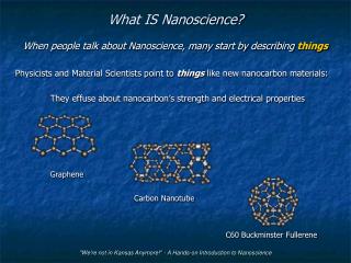
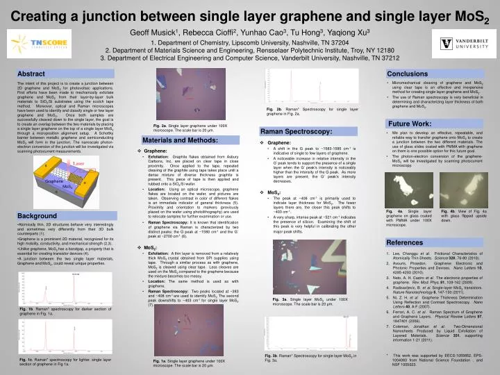
Creating a junction between single layer graphene and single layer MoS2 Geoff Musick1, Rebecca Cioffi2, Yunhao Cao3, Tu Hong3, Yaqiong Xu3 1. Department of Chemistry, Lipscomb University, Nashville, TN 37204 2. Department of Materials Science and Engineering, Rensselaer Polytechnic Institute, Troy, NY 12180 3. Department of Electrical Engineering and Computer Science, Vanderbilt University, Nashville, TN 37212 Abstract Laser Conclusions The intent of this project is to create a junction between 2D graphene and MoS2 for photovoltaic applications. First efforts have been made to mechanically exfoliate graphene and MoS2 from their layer-by-layer bulk materials to SiO2/Si substrates using the scotch tape method. Moreover, optical and Raman microscopes have been used to identify and classify single or few layer graphene and MoS2. Once both samples are successfully cleaved down to the single layer, the goal is to create an overlap between the two materials by placing a single layer graphene on the top of a single layer MoS2 through a microposition alignment setup. A Schottky barrier between metallic graphene and semiconducting MoS2 will form in the junction. The nanoscale photon-electron conversion of the junction will be investigated via scanning photocurrent measurements. • Micromechanical cleaving of graphene and MoS2 using clear tape is an effective and inexpensive method for creating single layer graphene and MoS2. • The use of Raman spectroscopy is very beneficial in determining and characterizing layer thickness of both graphene and MoS2. Fig. 2b. Raman* Spectroscopy for single layer graphene in Fig. 2a. Fig. 2a. Single layer graphene under 100X microscope. The scale bar is 20 μm. Materials and Methods: • Graphene: • Exfoliation: Graphite flakes obtained from Asbury Carbons, Inc. are placed on clear tape in close proximity. Once applied to the tape, repeated cleaving of the graphite using tape takes place until a dense mixture of diverse thickness graphite is present. This piece of tape is then applied and rubbed onto a SiO2/Si wafer. • Location: Using an optical microscope, graphene flakes are located on the wafer, and pictures are taken. Observing contrast in color of different flakes is an immediate indicator of general thickness (5). Proximity and orientation to markers (previously placed on the wafer using photolithography) are used to relocate samples for further examination or use. • Raman Spectroscopy:It is known that identification of graphene via Raman is characterized by two distinct peaks: the G peak at ~1580 cm-1 and the G` peak at ~2700 cm-1 (6). • MoS2: • Exfoliation: A thin layer is removed from a relatively thick MoS2 crystal obtained from SPI supplies using tape. Through a similar process as with graphene, MoS2 is cleaved using clear tape. Less cleaves are used on the MoS2 compared to the graphene because the mixture becomes too messy. • Location: The same method is used as with graphene. • Raman Spectroscopy: Two peaks located at ~383 and ~408 cm-1 are used to identify MoS2. The second peak downshifts to ~403 cm-1 for single layer MoS2 (7). Fig. 3b. Raman* Spectroscopy for single layer MoS2 in Fig. 3a. 520.27 Future Work: e-+h+ Fig. 3a. Single layer MoS2 under 100X microscope. The scale bar is 20 μm. • We plan to develop an effective, repeatable, and reliable way to transfer graphene onto MoS2 to create a junction between the two different materials. The use of glass slides coated with PMMA with graphene on them is one possible option for this future goal. • The photon-electron conversion of the graphene- MoS2 will be investigated by scanning photocurrent microscopy. Graphene MoS2 Background • Atomically thin, 2D structures behave very interestingly and sometimes very differently from their 3D bulk counterparts (1). • Graphene is a prominent 2D material, recognized for its high mobility, conductivity, and mechanical strength (2,3). • Unlike graphene, MoS2 has a bandgap, a property that is essential for creating transistor devices (4). • A junction between the two single layer materials, Graphene and MoS2, could reveal unique properties. Raman Spectroscopy: • Graphene: • A shift in the G peak to ~1583-1585 cm-1 is indicative of single to few layers of graphene. • A noticeable increase in relative intensity in the G’ peak tends to support the presence of a single layer when the G’ peak’s intensity is noticeably higher than the intensity of the G peak. As more layers are present, the G’ peak’s intensity decreases. • MoS2: • The peak at ~408 cm-1 is primarily used to indicate layer thickness for MoS2. The fewer layers there are, the closer this peak shifts to ~403 cm-1. • A very sharp, intense peak at ~521 cm-1 indicates the presence of silicon. Examining the shift of this peak is very helpful in calibrating the other major peak shifts. 1579.99 Fig. 4a. Single layer graphene on glass coated with PMMA under 100X microscope. Fig. 4b. View of Fig. 4a with glass flipped upside down. References 1. Lee, Changgu et al. Frictional Characteristics of Atomically Thin Sheets. Science328, 76-80 (2010). 2. Avouris, Phaedon. Graphene: Electronic and Photonic Properties and Devices. Nano Letters10, 4285-4293 (2010). 3. Neto, A. H. Castro et al. The electronic properties of graphene. Rev. Mod. Phys. 81, 109-162 (2009). 4. Radisavljevic, B. et al. Single-layer MoS2 transistors. Nature Nanotechnology6, 147-150 (2011). 5. Ni, Z. H. et al. Graphene Thickness Determination Using Reflection and Contrast Spectroscopy. Nano Letters40, A-F (2007). 6. Ferrari, A. C. et al. Raman Spectrum of Graphene and Graphene Layers. Physical Review Letters97, 1847401 (2006). 7. Coleman, Jonathan et al. Two-Dimensional Nanosheets Produced by Liquid Exfoliation of Layered Materials. Science331, supporting information 1-21 (2011). Fig. 1b. Raman* spectroscopy for darker section of graphene in Fig. 1a. Fig. 1a. Single layer graphene under 100X microscope. The scale bar is 20 μm. * This work was supported by EECS-1055852, EPS-1004083 from National Science Foundation , and NSF 1005023. Fig. 1c. Raman* spectroscopy for lighter, single layer section of graphene in Fig 1a.