Download
1 / 22
220 likes | 397 Views
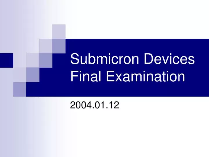
Submicron Devices Final Examination. 2004.01.12. Problem 1: Charge Sharing. Page 162, exercise 3.6. x j +ΔL. W dm. x j +W dm. (b). (a). Problem 2: Scaling. Please prove that the classical field scaling can maintain the constant power density (power/unit area).

E N D
Submicron DevicesFinal Examination 2004.01.12
Problem 1: Charge Sharing Page 162, exercise 3.6.
xj+ΔL Wdm xj+Wdm (b) (a)
Problem 2: Scaling • Please prove that the classical field scaling can maintain the constant power density (power/unit area). • Why does the constant field scaling not work for the small device. • If the E-field increases by a factor of α, how is the power density? Gate leakage is not considered.
(b) Why does the constant electrical field scaling not work for the small device? Main reason: In subthreshold region, Ioff is defined as Vg=0, Thus scaling down the threshold voltage Vt will result in increasing ofoff-current. Since we can not tolerate too large off-current, the scalingof Vt is limited, although the lower Vt can provide faster switching speed.
Problem 3: SOC for memory and logic For the same technology node. Make comparisons of Vt and Vdd for DRAM and Logic. What happens if DRAM and logic are integrated on the same chip? What are the challenges and possible solutions?
In DRAM technology, the off-current requirement is much more stringent forthe access transistor in the cell [Ioff(DRAM) << Ioff(Logic)], thus And for the purpose to keep the overdrive voltage, If DRAM and logic are integrated on the same chip:Considering two cases, 1. Vdd=Vdd(DRAM) It causes large electrical field in logic, and will result in problems of reliability. 2. Vdd=Vdd(Logic) It will result in too low overdrive voltage in DRAM, thus the switching speed of transistor in DRAM will be slow. Possible solution: use the process that allowed to adjust Vt so that we can obtain proper overdrive voltage.
Problem 4 Prove that for a symmetric doping profile, the effect on Vt are similar to a Delta profile with location corresponding to the symmetrical point and the dose corresponding to the integrated profile dose. The spreading doping has negligible effect on Vt, if the depletion region is wide enough.
Consider a simple symmetrical doping profile first, DI The electrical field distribution can be obtain by Poisson’s equation, And Vt is determined by surface field when Ψs=2ΨB
area increased = area decreased equivalent original The nonuniform step doping profile discussed above is equivalent to the delta-function profile with an equivalent dose of DI=(Ns-Na)xs centered atxc=xs/2 because both the area under ε(x) and εs are identical between the two cases. (εs is determined by the area under N(x) ) The similar arguments can be applied to any other symmetric profiles withsymmetric axis xc. Because the integral of symmetric profile (even function)is an odd function, the increased and decreased area under ε(x) (compared with the equivalent delta-function doping profile electrical field distribution) will be the same.
For example, considering a triangle symmetrical doping profile: area increased = area decreased DI equivalent N(x) Triangle profile xc xs x Wdm
Problem 5 If the device temperature increases from the room temperature, how is the Vt, mobility, and ID?
(a) Threshold voltage Vt Consider an nMOSFET with n+ polysilicon gate: …(A) From semiconductor physics, …(B) Substituting eq.(B) into eq.(A) we finally obtain, equals -1mV/K typically So
(b) mobility μi: Impurity scattering μph:Phonon scattering μsr:Surface roughness scattering Conclusion: T↑, impurity scattering↓, μi ↑ T↑, phonon scattering↑, μph ↓ T↑, interface roughness scattering↑, μsr ↓ (T>120K)(in general, interface roughness scattering is almost independent of T)Total effect: T↑ μeff ↓
(c) ID In saturation region,
Problem 6: Body effect Please derive the dependence for(a) uniform channel(b) extremely retrograded channel
(a) Uniform channel Consider the band diagram at the source terminal: When there is a reverse bias between bodyand source (VBS), the MOS structure is under non-equilibrium condition. Fermi level of electron and hole should be considered respectively: Efn : electron quasi-Fermi level Efp : hole quasi-Fermi level (almost unchanged) VBS As a result, surface inversion occurs when band bending : Thus the threshold voltage can be modified: Note that Vt is referred to the source, not body
(b) Extremely retrograded channel Consider general retrograded channel first,from Poisson’s equation: Channel doping Na xs Wdm x …(A) …(B) Substituting eq.(B) into eq.(A) and let to obtain Vt (referred to source) …(C) For extremely retrograded case (xs Wdm), Na must be high enough that to keep Wdm unchanged. We can expand eq.(C) under this limit to obtain (m is body-effect coefficient = 1+3tox / Wdm =1+3tox / xs for extremely retrograded case)
Problem 7: Dopant fluctuation Which location of the dopant fluctuation has more detrimental effect on Vt? Si/Oxide interface or depletion edge? Why?
We can treat fluctuation as a delta-function doping profile, and determineVt through the surface electrical field. (Vt is defined as Ψs=2ΨB ) Case1: fluctuation is near Si / oxide interface ε(x) fluctuation N(x) area increased = area decreased Δεs Total area = 2ΨB Wdm x x Wdm Case2: fluctuation is near depletion edge ε(x) fluctuation N(x) Total area = 2ΨB Δεs area increased = area decreased Wdm x x Wdm From above figure we can find that case1 has more effect on surface field,thus has more effect on Vt consequently.