Download
1 / 26
260 likes | 262 Views
This article discusses the current capabilities and future developments in flex hybrids, including technology drivers, speed, controlled impedance, materials, density, vias, thin dielectric materials, reliability, and more.

E N D
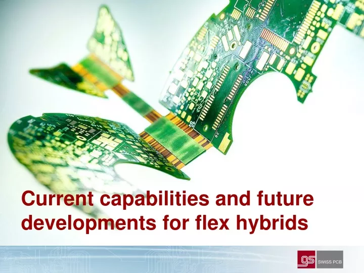
Current capabilities and future developments for flex hybrids
Author Dr. Frank Bose CEO GS Swiss PCB since 2002 • Low Energy Plasma Physics • RF engineering • Semiconductor Manufacturing • Equipment Manufacturing • PCB Manufacturing frank.bose@swisspcb.ch +41 41 854 4800
Table of Contents • Technology Drivers • Speed, High Frequency • Controlled Impedance • Materials, LCP • Density, Miniaturization • Pitch, Defect Density • Vias, Annular Ring • Thin dielectric materials • Reliability • Rigid-Flex • Plating • Metrology • (GS Roadmap • Other Developments • HicoFlex • Embedded Components (actives, passives and wave guides)
Clock Speed and RF Frequency • Ensure geometrical reproducibility of art work • Extract S-Parameters for better models and to account for parasitics • Find flex materials with good radio frequency properties • Material must posses good properties with respect to PCB manufacturing
Micro Strip Line Influence of geometrical variation on impedance
S-Parameter extraction required • Supplier value for er in FR4 is around 4.2-4.5 fitted values are closer to 3.7 ??? • Polar is de facto industry standard SW & measurement • Polar calculates around 1 MHz • Polar measurements done in time domain • S-Parameter extraction required for better models • Broader frequency range and parasitics • Skin effect & radiation due to treatment taken into account
Better flex materials required, i.e., LCP • Better mechanical stability • Low moisture absorption (stability, vacuum) • Better RF characteristics Tentzeris et al., IEEE Transactions on Microwave Theory and Techniques, Vol. 52, No.4, 2004
Example of LCP Substrates • LCP currently broadly used as high speed flex layer in hybrid build ups (LCP combined with other materials) • Full LCP build not readily available because of lamination problems, pattern dependence • Supply:Rogers, Nippon Steel (Espanex), and now Dupont
Density / Miniaturization • Main problem is isotropic nature of wet chemistry etching • Subtractive process vs additive process (panel plating vs pattern plating) • Stacked vias are reducing amount of real estate required for interconnects • Annular rings are required because of drill scatter even with CCD camera positioning • Defect density (defects per m2) is limiting availability of fine pitch PCBs
Subtractive Process • Easy process flow, economical • Pitch (p) limited top > 3*T T = Cu + resist thickness resist copper wanted reality laminate
Additive Process • Advanced process flow • Pattern dependence resist Seed copper plating etch laminate
Vias, Annular Ring and Catch Pad • Pads must be considerably larger than via diameter • Blind via must have aspect ratio > 1:1 • Stacked via enables real estate saving, no break-outs
What is limiting fine pitch processes? • Availability of thin seed layer materials (Hofstetter AG) • Defect density is not yet well controlled Currently 100mm pitch is available for small PCBs (3x3 cm)
Reliability & Metrology Stacked Vias expected to exhibit higher reliability • Base line and test in progress • Already used in implantable devices Metallization Problems • Plating is well understood • Choose a reliable vendor Full Flex and Rigid-flex • High reliability applications (aerospace) • Hearing Instrument hybrids as full – flex modules • Reduce interconnection complexity and connector failures
E-Test Polishing of Micro Section Micro Section Final Inspection 3D Image FAIR
Some other Developments • HiCoFlex (SHIFT, Hightec MC) • Embedded Components (VISA, HERMES, embedded chip (Würth, AT&S, Imbera, etc.) embedded interposer (Schweizer etc.) embedded passives • Embedded fibre-optics (Varioprint, PPC Cham) • Inkjet printed PCBs (cheap, but low performance)
HiCoFlex: Thin spin-on polyimide H. Burkhard, Hightec MC, Lenzburg, 6./7. September 2007
HiCoFlex • Spin-on polyimide film guaranties thin layer • Very fine etching possible due to sputtered seed layers • One sided assembly only • Panel size to increase from 6x6 inch to 12x24 • Single Source !
Embedded Die • Thermo-sonic flip chip embedded in PCB substrate • Laser cavity enables placement of thinned die R. Schönholz, Würth Schopfheim, Plus 2/2009, Leuze Verlag
Embedded Interposer • Lamination of interposer board into Multilayer • Testability, Known Good Interposer T. Gottwald et al., Schweizer Electronic AG, Plus 2/2009, Leuze Verlag
Embedded Passives • Resistive and capacitive layers within multilayer • Embedded ceramic components W.J. Borland et al., Dupont iTechnologies
Folded-in instead of embedded ! GS Swiss PCB / Phonak • Two layer flex PCB for flip chip (COF) • SiP for medical application • Polyimide thickness: 25 µm • Better testability of MCM • Better form factor as dielectric is thinner than standard pre-pregs • Easier supply chain integration • PCB yield does not push up electronics cost
Embedded Optical Waveguides Varioprint / IntexyS Photonics • Embedded polymer wave guide • High End Server backplane solution http://www.zurich.ibm.com/news/06/photonics_d.html
Summary • PCB technology is faced with the challenge of reducing the widening gap of silicon pitch and board pitch • Ever higher clock rates require precise artwork etching, often beyond current IPC Class 3 requirements • Reduction of foot print will evolve gradually, no revolutionary technology in sight • Material technology to evolve to include better RF properties, thinner dielectrics and thinner copper cladding • Increase in electrical function density to be expected with the use of embedded components, either active or passive, however, the jury is still out!