Download
1 / 36
390 likes | 638 Views
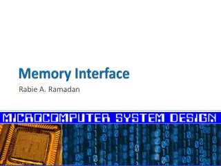
Memory is a device to store data To interfacing with memories, there must be: address bus, data bus and control (chip enable, output enable) To study memory interface, we must learn how to connect memory chips to the microprocessor and how to write/read data from the memory

E N D
Memory is a device to store data To interfacing with memories, there must be: address bus, data bus and control (chip enable, output enable) To study memory interface, we must learn how to connect memory chips to the microprocessor and how to write/read data from the memory Different kinds of memory chips will also be introduced Memory interface
Memory • Knowing memory is becoming more important • Your mobile devices do not have a harddisk but they have memory • IPad or other tablet computer has no harddisk! • But still very powerful! • Latest trend SSD (solid state drive) – a data storage device that uses solid-state memory to store data similar to a traditional harddisk • SSD is now rather expensive • A 64GB SSD is in the range HKD1000
Block diagram of a memory interface Address in Hex Content FFFF Data Control signals Include enable (chip select) , read/write 0000
Introduction • For the 8086 microprocessor, there are two modes: minimum and maximum • Under different modes, the memory interface is not the same • In the minimum mode, 8086 processor is connected to the external memory block directly • In the maximum mode, a Bus controller is needed • The bus controller will issue the required control signal to drive the memory block
Minimum Mode ALE memory 8086 /BHE /RD /WR M/IO DT//R /DEN A16-A19 AD0-AD15
Address space and data organization • Memory is organized as 8-bit bytes (byte as the basic unit) : one byte one address!!! • To address a word (16-bit) then 2 consecutive bytes are used, lower addressed byte is the LSB (Least Significant Byte) and the higher-addressed byte is the MSB (Most Significant Byte) • Words of data can be stored at even, or odd address boundaries 16-bit MSB LSB
Memory addressing • The address bit A0 of the LSBcan be used to determine the address boundary. If A0 is 0 then we have an even address, or aligned • If A0 is odd then we have odd-boundary • Example: 0001H is an odd-boundary address
Example • A0 = 1 example • A 16-bit data store at 01FFFH (then it is not aligned) and will occupy 01FFFH and 02000H (Odd boundary) • A0 = 0 example • A 16-bit data store at 02002H (then it is aligned) and will occupy 02002H and 02003H (even boundary)
Question • If you are asked to implement the memory system for a 8086 microprocessor, what memory configuration will you use? • One 1M Bytes chip • Two 512KBytes chips • One 1M Word chip √
Address Space • Even-boundary word can be accessed in one bus cycle • Odd-boundary word must be accessed in two bus cycle • In 8086, user’s data usually is in 8-bit or 16-bit format • For the system, instructions are always accessed as words (16-bit) • There is also double word format (32-bit)
Data type • Double word (32-bit) will be stored in 4 consecutive locations • When double word is used? • Double word can be used as a pointer that is used to address data or code outside the current segment • For a double word, the higher WORD stores the segment address, the lower WORD stores the offset
Memory organization 1M bytes memory using 2 512K byte chips Odd boundary Address requires 2 cycles BHE – bank high enable
Hardware organization • In hardware, the 1M bytes memory is implemented as two independent 512K-byte banks • Low (even) bank, and the high (odd) bank • Data from low bank use data bus 0-7 • Data from high bank use data bus 8-15 • Signal A0 enables the low bank • Signal /BHE enables the high bank • /BHE is active low • How many address lines are required in order to access 512K locations? (Ans. 19)
Memory organization Only A1 to A19 are used to drive the memory !!! High bank Low bank
Odd boundary • Consider the 16-bit word stored at 01233H then it occupy 01233H and 01234H • 01233H – 0000 0001 0010 0011 0011 • 01234H – 0000 0001 0010 0011 0100 • Only A1 to A19 are used to address the memory devices • Is it possible to active both addresses at the same time?
Odd-addressed word transfer Need two cycles! Odd address such as 1233H (low byte) + 1234H (high byte)
Example • Consider the 16-bit word stored at 01FFFH then it occupy 01FFFH and 02000H • In the first cycle data in 01FFFH will be read • In the second cycle data in 02000H will be read • Second case data stored in 02002H then data occupy 02002H and 02003H. Compare the bit pattern for 02002H and 02003H • 02002H – 0000 0010 0000 0000 0010 • 02003H – 0000 0010 0000 0000 0011 • Once again only consider A1 to A19 • Why both byte can be read in a single cycle?
Memory organization If data is stored in address 0H and 1H then both bytes can be read in a single cycle because bit0 is not used 000001 000000 000010 000001 High bank Low bank
Dedicated Memory locations Dedicated memory locations should not be used as general memory space for data and program storage For the 8086, address 00000 to 0007F and FFFF0 to FFFFB are dedicated Address from FFFFC to FFFFF are reserved
Exercise Determine the values for A0 and /BHE in order to access A byte at even address (/A0=0, /BHE = 1) A byte at odd address (/A0=1, /BHE = 0) A word at even address (aligned) (/A0=0, /BHE=0) A word at odd address (unaligned), as shown in the following figure (two cycles: First cycle get LSB /A0=1 /BHE=0 Second cycle get MSB /A0=0 /BHE =1 )
Memory control signals • To control the memory system in the minimum mode, requires: ALE, /BHE, M/IO, DT/R, /RD, /WR, and /DEN • ALE – address latch enable, signals external circuitry that a valid address is on the bus (0->1) so the address can be stored in the latch (or buffer) • M/IO – identify whether it is a memory or IO (Input/Output) operation (high – memory, low – I/O) • DT/R – transmit or receive (1 – transmit) • DEN – to enable the data bus
Read cycle of 8086 • Consists of 4 clock cycles • T1 – memory address is on the address bus, /BHE is also output, ALE is enable • Address is latch to external device at the trailing edge of ALE • T2 – M/IO and DT/R are set to 1 and 0 respectively. These signals remain their status during the cycle • Late in T2 - /RD is switched to 0 and /DEN also set to 0
Read cycle • T3 and T4 – status bits S3, S4 are output • Data are read during T3 • /RD and /DEN return to 1 at T4
Write cycle • T1 – address and /BHE are output and latched with ALE pulse • M/IO is set to 1, DT/R is also set to 1 • T2 - /WR set to 0 and data put on data bus • Data remain in the data bus until /WR returns to 1 • When /WR returns to 1 at T4, data is written into memory
Example • What is the duration of the bus cycle in the 8086-based microcomputer if the clock is 8MHz and two wait states are inserted Ans. 750ns (6 cycles) where each clock is 125ns
Demultiplexing the address/data bus • Address and data must be available at the same time when data are to be transferred over the bus • Address and data must be separated using external demultiplexing circuits (eg a latch, or buffer) • Address are latched into external circuits by ALE (address latch enable ) at T1
Demultiplexing the system bus One direction Bi-direction STB - Strobe Latches/buffers
Syntax to describe a memory • Memory is usually described by its size of storage and number of data bits • Eg. A 32K bytes memory chip is represented by 32Kx8 • A 32K bits memory is represented by 32Kx1
Configurations of memory for 16-bit data Chip enable (CE) usually generated by some decoding mechanism OE – output enable
Simple maths • From 00000H to FFFFFH there are 1M memory locations • How about from 0000H to FFFFH? • How many locations between 1FFFFFH to 310000H (answer in terms of M + K and Byte) • A memory system has 4M locations and the starting address is 420000H what is the ending address?
Memory architecture • Memory cells are usually organized in the form of an array • Each cell is capable of storing one bit of information. • Each row of cells constitutes a memory word, and all cells of a row are connected to a common line referred as the word line, controlledby the address decoder on the chip.
Memory architecture • The cells in each column are connected to a Sense/Write circuit by 2 bit lines, • The Sense/Write circuits are connected to the data input/output lines of the chip. • During a Read operation, these circuits sense, or read, the information stored in the cells selected by a word line and place this information on the output data lines. • During a Write operation, the Sense/Write circuits receive input data and store them in the cells of the selected word.