Download
1 / 23
230 likes | 255 Views
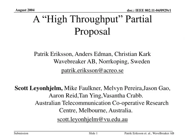
A High Density Small Size RF Test Module for High Throughput Multiple Resource Testing. Masayuki Kimishima ADVANTEST Corporation. Purpose. Trend of RF Test Increasing Test Ports of Devices Requirement for Low Test Cost . Requirements for RF ATE A Number of Simultaneous Measurement

E N D
A High Density Small Size RF Test Module for High ThroughputMultiple Resource Testing Masayuki Kimishima ADVANTEST Corporation
Purpose • Trend of RF Test • Increasing Test Ports of Devices • Requirement for Low Test Cost • Requirements for RF ATE • A Number of Simultaneous Measurement • Higher Throughput of RF Function Test • -Our Target of RF Module for ATE- • Full 4-cHResources Integration with Compact Size • High Throughput of RF Function Test
Outline • Comparison of New and Conventional RF Module • RF-SiP and RF board Construction • Core Technologies of RF-SiP - VNA Front-End SiP - High Speed SW Technology - RF Synthesizer SiP • Performance of New RF Module • Conclusion
Conventional RF Module ConstructionBased on “RF-HBIC and Coaxial Cable” • Circuit Construction • RF-HBIC • RF Interconnection • Coaxial Cable • Frequency Synthesizer • YIG-Tuned Oscillator • Signal SW and Attenuator Circuits • PIN Diode, or Conventional HEMT • Facing Difficulties in realization of • Multiple Resource Integration • Higher Throughput
New RF Module ConstructionBased on “RF-SiP and RF board” • Circuit Construction • RF-SiP • RF Interconnection • BGA & RF board • Frequency Synthesizer • SiP Integration by PLL-LSI • Signal SW and Attenuator Circuits • High Speed SW and ATT MMICs • Achievement of Compact RF Module with • Full 4-cH Multiple Resources • Higher Throughput per cH
Structure of New RF Module Each Boards for 4-cH Volume Corresponds to“ 1/15 ” with Conventional Structure
Can Operate Each of 4-cH Individually Resource Construction of RF Module New RF Module Conventional RF Module
Outline • Comparison of New and Conventional RF Module • RF-SiP and RF board Construction • Core Technologies of RF-SiP - VNA Front-End SiP - High Speed SW Technology - RF Synthesizer SiP • Performance of New RF Module • Conclusion
Structure of RF-SiP ALL SiPs are the same size of 20mm sq.
RF Front-End Diagram for One Channel RF Front-End Board RF Synthesizer Board
Outline • Comparison of New and Conventional RF Module • RF-SiP and RF board Construction • Core Technologies of RF-SiP - VNA Front-End SiP - High Speed SW Technology - RF Synthesizer SiP • Performance of New RF Module • Conclusion
Measured Data of VNA-FE SiP Accuracy Conversion Gain and Noise Figure Dynamic range@1MHz BW, Freq-input : 2GHz = Pin_max - (Floor Noise + NF + Gain) - BW = + 10 - (-174 + 38 - 10) - 60 = 96 dB
Outline • Comparison of New and Conventional RF Module • RF-SiP and RF board Construction • Core Technologies of RF-SiP - VNA Front-End SiP - High Speed SW Technology - RF Synthesizer SiP • Performance of New RF Module • Conclusion
Settling Time of HEMT Device Definition of Settling Time Our Definition is 0 to 99.9% (0.01dB) Comparison of Settling Time for HEMTs
This Work Conventional HEMT Measurement Great Improvement on Settling Time Simulation Measured Data of SP4T Switch MMIC Frequency Characteristics Settling Time
Outline • Comparison of New and Conventional RF Module • RF-SiP and RF board Construction • Core Technologies of RF-SiP - VNA Front-End SiP - High Speed SW Technology - RF Synthesizer SiP • Performance of New RF Module • Conclusion
Block Diagram of RF Synthesizer SiP(Fractional-N Frequency Synthesizer) 13 VCOs PLL-LSI
Measured Data of Multi-Band VCOs(Frequency Response & Phase Noise) @ 1MHz off carrier
Fraction Integer 48-bit, 4th-Order MASH Architecture - Step Size < 100 uHz - Quantization Noise Shaping Around 400kHz Loop BW Integer Fraction Block Diagram of Fractional-N Frequency Divider
Outline • Comparison of New and Conventional RF Module • RF-SiP and RF board Construction • Core Technologies of RF-SiP - VNA Front-End SiP - High Speed SW Technology - RF Synthesizer SiP • Performance of New RF Module • Conclusion
Performance of New RF Module Dynamic Range of VSG Frequency Settling Time of VSG < 150 usec Conventional : 800 usec
Conclusion Compact Size RF Test Module with • Full 4-cH Resource Integration • Using RF-SiP and RF board Instead of Hybrid-IC and Coaxial Cable • Elimination of YIG Oscillator and PIN-Diode Switch • High Throughput of RF Function Test • High Speed Switch/Attenuator MMIC • VCO Base RF Synthesizer