Download
1 / 4
40 likes | 42 Views
In this paper we have produced NiO thin film based solar cells. The NiO thin film was then studied for their structural, optical and electrical properties. By the help of these results we have capable to know about the structure of NiO the phase purity of the thin film X ray diffraction XRD pattern of NiO showed the diffraction planes corresponding to cubic phase respectively. The optical properties showed that with the increase in the deposition time of NiO the energy band gap varied between 3.1 to 3.24 eV. In the end, IV characteristics of the thin films were obtained by the help of matlab in the presence of light as will as dark region. Vijay Aithekar "An Research Article on Fabrication and Characterization of Nickel Oxide Coated Solar Cell" Published in International Journal of Trend in Scientific Research and Development (ijtsrd), ISSN: 2456-6470, Volume-3 | Issue-5 , August 2019, URL: https://www.ijtsrd.com/papers/ijtsrd25300.pdf Paper URL: https://www.ijtsrd.com/physics/nanotechnology/25300/an-research-article-on-fabrication-and-characterization-of-nickel-oxide-coated-solar-cell/vijay-aithekar<br>

E N D
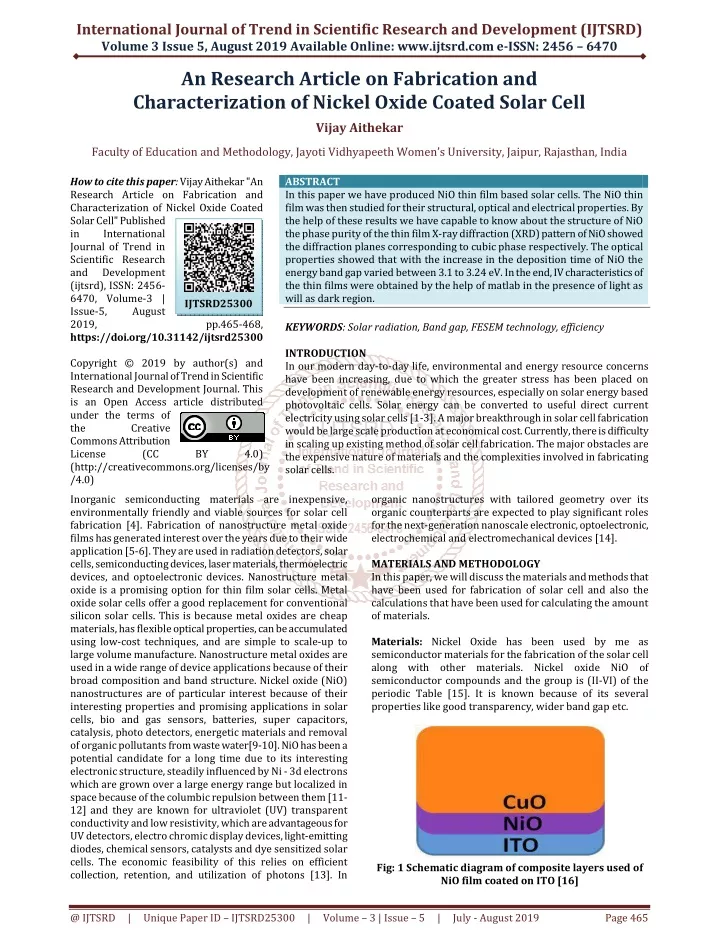
International Journal of Trend in Scientific Research and Development (IJTSRD) Volume 3 Issue 5, August 2019 Available Online: www.ijtsrd.com e-ISSN: 2456 – 6470 An Research Article on Fabrication and Characterization of Nickel Oxide Coated Solar Cell Vijay Aithekar Faculty of Education and Methodology, Jayoti Vidhyapeeth Women’s University, Jaipur, Rajasthan, India How to cite this paper: Vijay Aithekar "An Research Article on Fabrication and Characterization of Nickel Oxide Coated Solar Cell" Published in International Journal of Trend in Scientific Research and Development (ijtsrd), ISSN: 2456- 6470, Volume-3 | Issue-5, August 2019, https://doi.org/10.31142/ijtsrd25300 Copyright © 2019 by author(s) and International Journal of Trend in Scientific Research and Development Journal. This is an Open Access article distributed under the terms of the Creative Commons Attribution License (CC (http://creativecommons.org/licenses/by /4.0) Inorganic semiconducting materials are inexpensive, environmentally friendly and viable sources for solar cell fabrication [4]. Fabrication of nanostructure metal oxide films has generated interest over the years due to their wide application [5-6]. They are used in radiation detectors, solar cells, semiconducting devices, laser materials, thermoelectric devices, and optoelectronic devices. Nanostructure metal oxide is a promising option for thin film solar cells. Metal oxide solar cells offer a good replacement for conventional silicon solar cells. This is because metal oxides are cheap materials, has flexible optical properties, can be accumulated using low-cost techniques, and are simple to scale-up to large volume manufacture. Nanostructure metal oxides are used in a wide range of device applications because of their broad composition and band structure. Nickel oxide (NiO) nanostructures are of particular interest because of their interesting properties and promising applications in solar cells, bio and gas sensors, batteries, super capacitors, catalysis, photo detectors, energetic materials and removal of organic pollutants from waste water[9-10]. NiO has been a potential candidate for a long time due to its interesting electronic structure, steadily influenced by Ni - 3d electrons which are grown over a large energy range but localized in space because of the columbic repulsion between them [11- 12] and they are known for ultraviolet (UV) transparent conductivity and low resistivity, which are advantageous for UV detectors, electro chromic display devices, light-emitting diodes, chemical sensors, catalysts and dye sensitized solar cells. The economic feasibility of this relies on efficient collection, retention, and utilization of photons [13]. In ABSTRACT In this paper we have produced NiO thin film based solar cells. The NiO thin film was then studied for their structural, optical and electrical properties. By the help of these results we have capable to know about the structure of NiO the phase purity of the thin film X-ray diffraction (XRD) pattern of NiO showed the diffraction planes corresponding to cubic phase respectively. The optical properties showed that with the increase in the deposition time of NiO the energy band gap varied between 3.1 to 3.24 eV. In the end, IV characteristics of the thin films were obtained by the help of matlab in the presence of light as will as dark region. KEYWORDS: Solar radiation, Band gap, FESEM technology, efficiency INTRODUCTION In our modern day-to-day life, environmental and energy resource concerns have been increasing, due to which the greater stress has been placed on development of renewable energy resources, especially on solar energy based photovoltaic cells. Solar energy can be converted to useful direct current electricity using solar cells [1-3]. A major breakthrough in solar cell fabrication would be large scale production at economical cost. Currently, there is difficulty in scaling up existing method of solar cell fabrication. The major obstacles are the expensive nature of materials and the complexities involved in fabricating solar cells. IJTSRD25300 pp.465-468, BY 4.0) organic nanostructures with tailored geometry over its organic counterparts are expected to play significant roles for the next-generation nanoscale electronic, optoelectronic, electrochemical and electromechanical devices [14]. MATERIALS AND METHODOLOGY In this paper, we will discuss the materials and methods that have been used for fabrication of solar cell and also the calculations that have been used for calculating the amount of materials. Materials: Nickel Oxide has been used by me as semiconductor materials for the fabrication of the solar cell along with other materials. Nickel oxide NiO of semiconductor compounds and the group is (II-VI) of the periodic Table [15]. It is known because of its several properties like good transparency, wider band gap etc. Fig: 1 Schematic diagram of composite layers used of NiO film coated on ITO [16] @ IJTSRD | Unique Paper ID – IJTSRD25300 | Volume – 3 | Issue – 5 | July - August 2019 Page 465
International Journal of Trend in Scientific Research and Development (IJTSRD) @ www.ijtsrd.com eISSN: 2456-6470 The microstructures of the NiO thin layer has investigated by state-of-the-art techniques like X-ray diffractometer (XRD, Brucker D2 Phaser system) with Cu Kα radiation operating at 30 kV and 10 mA having wavelength of 0.154 nm under out-of-plane geometry. For the morphological analysis, Scanning Electron Microscopy has carried out for nanostructure analysis of such inorganic layers. The optical transmission/absorption spectra of the samples have obtained in the ultraviolet (UV)/Visible/near infrared (NIR) region up to 1100 nm using Shimazdu UV-VIS spectrophotometer. These kinds of properties make it as a good option to be use for fabrication of PV devices. For the measurement of surface morphology, field emission scanning electron microscopy (FE-SEM; model: JEOL JSM- 7600F) with accelerating voltage of 5 kV has use. The film thickness has measure using surface profiler (model: Veeco Dektak 750) while to observe transmittance and absorbance, ultraviolet-visible spectroscopy (UV-VIS; model: JASCO V- 670) has use. The electrical properties of the NiO thin films were measured by Ecopia HMS-3000 Hall system. All the measurements were performed at room temperature. Results and discussion crystal structure to investigate the crystal quality of the NiO thin film. RESULTS AND DISCUSSIONS In this section, results obtained by applying different characterization techniques on our sample will be discussed. X-Ray Diffraction, Scan Electron Microscopy and IV characteristics of our sample have been done and in this chapter their results will be shared. 1.OPTICAL PROPERTY: Nickel oxide (NiO) has cubic (NaCl-like FCC) structure and pale green colour. And has a crystalline structure of the rock salt kind of structure of sodium chloride salt (NaCl). The stoichiometry of NiO is roughly indicated by the color of the sample. The color f the NiO is highly sensitive to the presence of higher valence states of nickel even in traces. NiO exhibits wide band gap energy within the UV region in the range of 3.5– 4.0eV at room temperature. Nano-particles of Nickel oxide are transparent to the visible spectrum of solar radiations. When ultra violet spectrum of light falls on the NiO material it absorbs almost all part of the UV light and it act as a transparent medium allowing the visible light to pass through it. The optical transmittance of all as-prepared NiO thin films is more than 60 % at the visible range, shown in Fig.2. The transmittance of the films decreased from 90 % to 65% with the increase of sputtering power from 50 to 150 W. measurements were performed on NiO thin films, shown in Fig.4. Indicates the presence of NiO (111), NiO (200), NiO (220) as well as NiO (311) peaks, where NiO (111) and NiO (200) are the pronounced peaks. The XRD analysis confirms Bunsenite, which corresponds to the JCPDS card: 04-0835 for nickel oxide [40] confirming it as a good absorber layer of solar cells. Fig: 4 XRD pattern of NiO All the indexed peaks obtained in the XRD of the sample were exactly the same as of reference card peaks and were matched accordingly this also shows that our sample is phase pure. The result obtained shows that our NiO particles were 100% phase pure. 3.SEM of NiO Particles: The surface morphology variation of NiO thin films with sputtering power was observed by SEM, shown in Fig.5 Fig: 5 FESEM of NiO particles All samples had a columnar structure with growth perpendicular to the film surface, and were dense, and homogeneous. With the increase of sputtering power, the grain surface was obtained. It may be attributed to the transformation of thin film growth model. When the sputtering power is low, the basic unit of film growth is less; film growth appears to island growth mode. Gradually increases from a size of 10 to 50 nm. With the increase of the sputtering power, the basic unit required for film growth also increased, and the islands on substrate gradually increase. The thickness of NiO thin film deposited at various sputtering power was given in Fig.6. We observed that the thickness of NiO thin films linearly increases with the increase of sputtering power. Fig: 2 Cubic structure of Nickle Oxide 2.XRD of NiO Particles: To investigate the crystal quality of the NiO thin films prepared at different sputtering power, X-ray diffraction Fig: 6 3D analytical image of NiO @ IJTSRD | Unique Paper ID – IJTSRD25300 | Volume – 3 | Issue – 5 | July - August 2019 Page 466
International Journal of Trend in Scientific Research and Development (IJTSRD) @ www.ijtsrd.com eISSN: 2456-6470 4.IV Characteristics: The IV characterization can be done either in outdoor conditions in which solar cell is exposed to sun light and solar radiations directly fall on the subject solar cell and we measure the reading by the use of millimeter or in indoor conditions in which sample solar cell is exposed to the sun simulator and accordingly readings of the current and voltage are measured. Outdoor measurement method tells us the actual efficiency of the solar cell. Following solar cell parameters are kept in mind while analyzing the IV characteristics of a solar cell- Short-Circuit Current Density (Jsc): Jscis the current that flows through the junction under illumination at zero applied voltage, that is, Jsc = J (V = 0). In the ideal case, it equals the photo generated current density (Jl) and is proportional to the incident number of photons or alternatively the intensity of illumination [17]. Jsc = Jo [exp {q(0) /AkT}-1] – Jv ,V=0 Open Circuit Voltage (Voc): It is defined as the maximum voltage available at the output of a solar cell when the current is zero. The open circuit voltage can be derived by using the following equation [18]. Voc = AkT /q ln (Ii/Io + 1) Fill Factor: In addition to open circuit voltage and short circuit current, the fill factor also determines the maximum amount of power from a solar cell. Mathematically it is a ratio of Voc and Isc. High fill factor means that the solar cell has less series resistance and has high shunt resistance so there is less dissipation in internal losses. FF = Pmax/VocIsc Efficiency: Efficiency of a solar cell depends upon the intensity of solar radiations and temperature of the solar cell. Terrestrial solar cells are measured in AM 1.5 conditions and at ISO temperature of 25 0C. It is basically defined as the “fraction of incident power that is being converted to electricity”. Efficiency is calculated by using following formula [20]. η = JscVocFF/Pin The IV curve obtained after performing the results shows a type of linear graph in both dark and in light region. open-circuit voltage, short-circuit current, and fill factor were 2.30%, 350 mV, 16.8 mA, and 69% under illumination, respectively. This is an improvement on existing values. This will open up frontiers in affordable and sustainable solar cell fabrication in developing and low-income countries. References [1]Chu, Y. and Meisen, P. (2011) Review and Comparison of Different Solar Energy Technologies. Report of Global Energy Network Institute (GENI), Diego. [2]McEvoy, A., Castaner, L. and Markvart, T. (2012) Solar Cells: Materials, Manufacture and Operation. 2nd Edition, Elsevier Ltd., Oxford, 3-25. [3]Shruti Sharma, Kamlesh Kumar, “Solar Cells: In Research and Applications – A Review”, Materials Sciences and Applications, page 1145-1155, 2015. [4]M. Zaheer, “Solar Raidation Measurements for Solar Energy Applications”, Kipp and Zonen, 2015. [5]S. Joshi, M. Mudigere, L. Krishnamurthy, and G. Shekar, “Growth and morphological studies of NiO/CuO/ZnO based nanostructured thin films for photovoltaic applications,” Chemical Papers, vol. 68, no. 11, pp. 1584–1592, 2014. [6]B. A. Reguig, A. Khelil, L. Cattin, M. Morsli, J.C. Berne`de " Properties of NiO thin films deposited by intermittent spray pyrolysis process", Applied Surface Science, Vol. 253, pp. 4330–4334, (2007 [7]G. Benedek, L. Reining, M. Gatti," Exchange and Correlation effects in the electronic properties of transition metal oxides: the example of NiO ", Anno Accademico, (2008). [8]M. Guziewicza, W. Junga, J. Grochowskia, M. Borysiewicza, K Golaszewskaa, R. Kruszkaa, A. Baranskaa, A. Piotrowskaa, B.S. Witkowskib, J.Z. Domagalaa;b,M. Gryzinskic, K. Tyminskac and A. Stonertd, aInstitute of Electron Technology, al. Lotników ,Vol.120, 32/46, 02-668, Poland, (2012). [9]B. A. Reguig, A. Khelil, L. Cattin, M. Morsli, J. C. Berne`de " Properties of NiO thin films deposited by intermittent spray pyrolysis process", Applied Surface Science, Vol. 253, pp. 4330–4334, (2007) . [10]Hiroki Kidowaki, Takeo Oku, Tsuyoshi Akiyama, Atsushi Suzuki, Balachandran Jeyadevan, Jhon Cuya. Fabrication and Characterization of CuO-based Solar Cells Journal of Materials Science Research 2012;1 (1): 138-143. [11]F. Bayansal, H.A. C¸ etinkara, S. Kahraman, H.M. C¸ akmak, H.S. Gu¨der "Nano-structured CuO films prepared by simple solution methods: Plate-like, needle-like and network-like architectures",Ceramics International, Vol. 38, pp.1859–1866, (2012). [12]Ratnesh Sharma, A.D. Acharya, S.B. Shrivastava, T. Shripath and V. Ganesan," characterization of transparent NiO thin films deposited by spray pyrolysis technique",Optik,Vol. 125, pp. 6751–6756, (2014). Preparation and CONCLUSION In this study, NiO thin films were used to fabricate NiO heterojunction solar cells. It shows that NiO can be used in thin-film solar cells. The result of conversion efficiency, [13]T. Shinagawa, M. Chigane, J. Tani, and M. Izaki, “Effect of oxide intermediate layers on pyramidally textured Cu2O/ ZnO solar cells prepared by electrodeposition,” ECS Meeting Abstracts, vol. 2, no. 21, p. 1636, 2016. @ IJTSRD | Unique Paper ID – IJTSRD25300 | Volume – 3 | Issue – 5 | July - August 2019 Page 467
International Journal of Trend in Scientific Research and Development (IJTSRD) @ www.ijtsrd.com eISSN: 2456-6470 [14]A. Samad, M. Furukawa, H. Katsumata, T. Suzuki, and S. Kaneco, “Photocatalytic oxidation and simultaneous removal of arsenite with CuO/ZnO photocatalyst,” Journal of Photochemistry and Photobiology A: Chemistry, vol. 325, pp. 97–103, 2016. [17]Balchandara Chikate, Y.A. Sadawatre, “Factors Affecting the Performance of Solar Cells”, International Journal of Computer Applications, 2015. [18]M. Y. Levy and Honsberg, C. B., “Rapid and precise calculations of energy and particle flux for detailed- balance photovoltaic Electronics, vol. 50, pp. 1400-1405, 2006. [15]E. Fujii, A. Tomozawa, H. Torii, and R. Takayama, “Preferred orientations of NiO films prepared by plasma-enhanced metalorganic deposition, ”Japanese Journal of Applied Physics, Vol. 35, pp. L328–L330, (1996). applications”, Solid-State chemical vapor [19]M. A. Green, “Solar cell fill factors: General graph and empirical expressions”, Solid-State Electronics, vol. 24, pp. 788 - 789, 1981. [16]P. Potapov and D. Schryvers, EMAT, University of Antwerp, RUCA, Groenenborgerlaan 171, B-2020 Antwerp, Belgium, Physical Reviewb, 69, 184404 (2004). [20]M. A. Green, “Accuracy of Analytical Expressions for Solar Cell Fill Factors”, Solar Cells, vol. 7, pp. 337-340, 1982. @ IJTSRD | Unique Paper ID – IJTSRD25300 | Volume – 3 | Issue – 5 | July - August 2019 Page 468