Download
1 / 5
50 likes | 54 Views
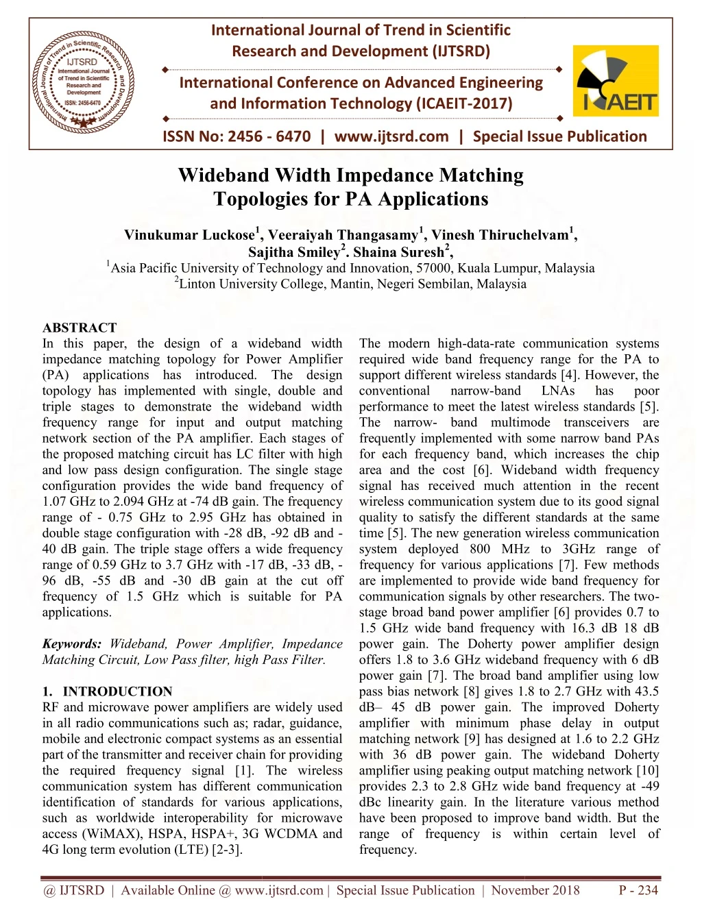
In this paper, the design of a wideband width impedance matching topology for Power Amplifier PA applications has introduced. The design topology has implemented with single, double and triple stages to demonstrate the wideband width frequency range for input and output matching network section of the PA amplifier. Each stages of the proposed matching circuit has LC filter with high and low pass design configuration. The single stage configuration provides the wide band frequency of 1.07 GHz to 2.094 GHz at 74 dB gain. The frequency range of 0.75 GHz to 2.95 GHz has obtained in double stage configuration with 28 dB, 92 dB and 40 dB gain. The triple stage offers a wide frequency range of 0.59 GHz to 3.7 GHz with 17 dB, 33 dB, 96 dB, 55 dB and 30 dB gain at the cut off frequency of 1.5 GHz which is suitable for PA applications. Vinukumar Luckose | Veeraiyah Thangasamy | Vinesh Thiruchelvam | Sajitha Smiley | Shaina Suresh "Wideband Width Impedance Matching Topologies for PA Applications" Published in International Journal of Trend in Scientific Research and Development (ijtsrd), ISSN: 2456-6470, Special Issue | International Conference on Advanced Engineering and Information Technology , November 2018, URL: https://www.ijtsrd.com/papers/ijtsrd19148.pdf Paper URL: https://www.ijtsrd.com/engineering/electronics-and-communication-engineering/19148/wideband-width-impedance-matching-topologies-for-pa-applications/vinukumar-luckose<br>

E N D
International Journal of Trend in Scientific Research and International Conference on Advanced Engineering and Information Technology (ICAEIT-2017) deband Width Impedance Matching Topologies for PA Applications International Journal of Trend in Scientific Research and Development (IJTSRD) International Conference on Advanced Engineering and Information Technology (ICAEIT ISSN No: 2456 - 6470 | www.ijtsrd.com | Special Issue Publication International Conference on Advanced Engineering ISSN No: 2456 Special Issue Publication Wideband Width Impedance Matching Topologies Vinukumar Luckose1, Veeraiyah Thangasamy Sajitha Smiley 1Asia Pacific University of Technology and Innovation, 57000, Kuala Lumpur, Malaysia 2Linton University College, Mantin, Negeri Sembilan, Malaysia Linton University College, Mantin, Negeri Sembilan, Malaysia Linton University College, Mantin, Negeri Sembilan, Malaysia , Veeraiyah Thangasamy1, Vinesh Thiruchelvam Sajitha Smiley2. Shaina Suresh2, Asia Pacific University of Technology and Innovation, 57000, Kuala Lumpur, Malaysia Asia Pacific University of Technology and Innovation, 57000, Kuala Lumpur, Malaysia Thiruchelvam1, ABSTRACT In this paper, the design of a wideband width impedance matching topology for Power Amplifier (PA) applications has introduced. The design topology has implemented with single, double and triple stages to demonstrate the wideband width frequency range for input and output matching network section of the PA amplifier. Each stages of the proposed matching circuit has LC filter with high and low pass design configuration. The single stage configuration provides the wide band frequency of 1.07 GHz to 2.094 GHz at -74 dB gain. The frequency range of - 0.75 GHz to 2.95 GHz has obtained in double stage configuration with -28 dB, 40 dB gain. The triple stage offers a wide frequency range of 0.59 GHz to 3.7 GHz with -17 dB, 96 dB, -55 dB and -30 dB gain at the cut off frequency of 1.5 GHz which is suitable for PA applications. Keywords: Wideband, Power Amplifier, Impedance Matching Circuit, Low Pass filter, high Pass Filter. 1.INTRODUCTION RF and microwave power amplifiers are widely used in all radio communications such as; radar, guidance, mobile and electronic compact systems as an essential part of the transmitter and receiver chain for providing the required frequency signal [1]. The wi communication system has different communication identification of standards for various applications, such as worldwide interoperability for microwave access (WiMAX), HSPA, HSPA+, 3G WCDMA and 4G long term evolution (LTE) [2-3]. The modern high-data-rate communication systems required wide band frequency range for the PA to support different wireless standards [4]. However, the conventional narrow-band performance to meet the latest wireless standards [5]. The narrow- band multimode frequently implemented with some narrow band PAs for each frequency band, which area and the cost [6]. Wideband width frequency signal has received much attention in the recent wireless communication system due to its go quality to satisfy the different standards at time [5]. The new generation wireless communication system deployed 800 MHz to 3GHz range of frequency for various applications [7]. Few methods are implemented to provide wide band frequency communication signals by other researchers. The two stage broad band power amplifier [6] provides 0.7 to 1.5 GHz wide band frequency with power gain. The Doherty power amplifier design offers 1.8 to 3.6 GHz wideband frequency with 6 dB power gain [7]. The broad band amplifier using low pass bias network [8] gives 1.8 to 2.7 GHz with 43.5 dB– 45 dB power gain. The improved Doherty amplifier with minimum phase delay in output matching network [9] has designed at 1.6 to 2.2 GHz with 36 dB power gain. The wideband Doherty amplifier using peaking output matching network [10] provides 2.3 to 2.8 GHz wide band frequency at dBc linearity gain. In the literature various method have been proposed to improve band width. But the range of frequency is within certain level of frequency. In this paper, the design of a wideband width impedance matching topology for Power Amplifier (PA) applications has introduced. The design topology has implemented with single, double and triple stages to demonstrate the wideband width ange for input and output matching network section of the PA amplifier. Each stages of the proposed matching circuit has LC filter with high and low pass design configuration. The single stage configuration provides the wide band frequency of rate communication systems required wide band frequency range for the PA to support different wireless standards [4]. However, the band performance to meet the latest wireless standards [5]. band multimode transceivers are frequently implemented with some narrow band PAs for each frequency band, which increases the chip [6]. Wideband width frequency signal has received much attention in the recent wireless communication system due to its good signal quality to satisfy the different standards at the same generation wireless communication system deployed 800 MHz to 3GHz range of frequency for various applications [7]. Few methods are implemented to provide wide band frequency for communication signals by other researchers. The two- stage broad band power amplifier [6] provides 0.7 to 1.5 GHz wide band frequency with 16.3 dB 18 dB power gain. The Doherty power amplifier design offers 1.8 to 3.6 GHz wideband frequency with 6 dB ower gain [7]. The broad band amplifier using low pass bias network [8] gives 1.8 to 2.7 GHz with 43.5 45 dB power gain. The improved Doherty amplifier with minimum phase delay in output [9] has designed at 1.6 to 2.2 GHz LNAs LNAs has has poor poor 74 dB gain. The frequency 0.75 GHz to 2.95 GHz has obtained in 28 dB, -92 dB and - 40 dB gain. The triple stage offers a wide frequency 17 dB, -33 dB, - 30 dB gain at the cut off frequency of 1.5 GHz which is suitable for PA Wideband, Power Amplifier, Impedance Matching Circuit, Low Pass filter, high Pass Filter. RF and microwave power amplifiers are widely used in all radio communications such as; radar, guidance, mobile and electronic compact systems as an essential part of the transmitter and receiver chain for providing the required frequency signal [1]. The wireless communication system has different communication identification of standards for various applications, such as worldwide interoperability for microwave access (WiMAX), HSPA, HSPA+, 3G WCDMA and The wideband Doherty amplifier using peaking output matching network [10] provides 2.3 to 2.8 GHz wide band frequency at -49 dBc linearity gain. In the literature various method have been proposed to improve band width. But the is within certain level of @ IJTSRD | Available Online @ www.ijtsrd.com | Special Issue Publication | November 2018 @ IJTSRD | Available Online @ www.ijtsrd.com | Special Issue Publication | November 2018 @ IJTSRD | Available Online @ www.ijtsrd.com | Special Issue Publication | November 2018 P - 234
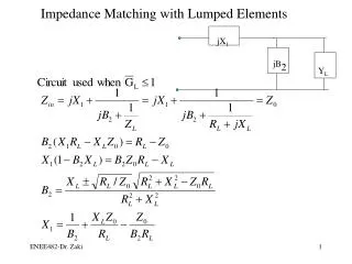
International Journal of Trend in Scientific Research and Development (IJTSRD) | ISSN: 2456-647 In this paper input and output impedance matching network topologies has designed for power amplifier application to obtain wide band frequency. The proposed work is designed with single, double and triple stage impedance matching circuit with High- Low and Low- High cascaded configuration. Each stages are embedded with high pass and low pass filter network. The triple stage impedance matching topology achieved with 0.6 to 3.75 GHz wide band frequency. 2.Design Methodology: Figure 1 shows the block diagram of basic impedance matching network configuration with power amplifier stage. In the high-low input-matching network, the transformation ratio has 50 Ω to 1.85 Ω while the output-matching network low-high used with 1.85 Ω to 50 Ω. The input and output matching network has designed with the combination of High and Low pass cascaded configuration. cascaded with another three-stage low pass filter. The impedance matching levels has designed with the impedance transformation from 50 Ω to 1.85 Ω. In three stage cascaded network the matching levels are thus 50 Ω, 28.82 Ω, 16.66 Ω, 9.62 Ω, 5.55 Ω 3.207 Ω and 1.85Ω. Figure2. Single stage High – Low Matching Circuit Figure3. Double stage High – low matching circuit Figure1. Basic Impedance Matching Block Diagram 2.1 High-Low cascaded network design for Input matching circuit: The single stage high-low impedance matching network is shown in Figure 2. The components L1 and C1 act as high pass filter and L2, C2 act as Low pass filter. The source (Rs) has the impedance of 50 Ω and the load resistance is 1.85 Ω. In the single stage, the matching levels are thus 50 Ω, 9.62 Ω and 1.85 Ω. The impedance transformation ratio is 27 to one and this is achieved by cascading the high and low pass impedance transformation to one. The value of inductor (L) and capacitor (C) has designed using the matching levels of the circuit. The impedance matching calculations has done at a center of frequency of 1.5 GHz. Figure 3 shows the double stage impedance matching network. The L1, L2 and C1, C2 act as high pass filter; L3, L4 and C3, C4 act as low pass filter. The impedance matching levels are thus 50 Ω, 21.92 Ω, 9.61 Ω, 4.21 Ω and 1.85 Ω used in double stage matching network. Triple stage high- low impedance matching network is shown in Figure 4. The circuit has designed with three high pass filter Figure4. Triple stage High-Low matching Circuit 2.2 Low-High cascaded network design for output matching circuit: The design steps for Low-High impedance matching networks has discussed below. The impedance matching network shown in Figure 5 is the single stage network with the components L1 and C1 act as low pass filter and L2, C2 act as high pass filter. The transformation ratio has 50 Ω to 1.85 Ω. The matching network has designed with the same value of Q as used in High-low matching network. The matching levels are thus 1.85 Ω, 9.62 Ω and 50 Ω. The impedance matching calculations has done at a @ IJTSRD | Available Online @ www.ijtsrd.com | Special Issue Publication | November 2018 P - 235
International Journal of Trend in Scientific Research and Development (IJTSRD) | ISSN: 2456-647 center of frequency of 1.5 GHz. The double stage low- high impedance matching network has shown in Figure6. The L1, L2 and C1, C2 act as low pass filter; L3, L4 and C3, C4 act as high pass filter. The impedance matching levels are thus 1.85 Ω, 4.21 Ω, 9.61 Ω, 21.92 Ω and 85 Ω used in double stage matching network. Figure 7 shows the Triple stage low-high impedance matching network. Three low pass filter cascaded with another three-stage high pass filter for obtaining the wideband frequency. The matching levels are thus 1.85Ω, 3.20 Ω, 5.55 Ω, 9.62 Ω, 16.6 Ω, 28.82 Ω and 50 Ω used in triple stage matching network. 3.1 Simulation Results for High-Low Cascaded Network for input matching circuit: In this section the High-Low impedance matching network for single, double and triple stage has discussed. The single stage High-Low matching circuit is shown in Figure 8. The matching circuit has achieved a widebandwith frequency range of 1.2 GHz to 2.2 GHz with the cut of frequency of 1.5 GHz. The gain of the single stage matching circuit has -73 dB. The Q factor value for the single stage has 2.048. The Double stage High-Low matching circuit as shown in Figure 9 has obtained the wide band frequency band of 0.7 GHz to 2.9 GHz with the same cut off frequency. The gain values are obtained at -29 dB, -93 dB and -47 dB with the cut off frequency of 1.5 GHz. The larger wide band frequency has obtained in the triple stage impedance matching circuit as shown in Figure 10. The range of frequency is from 0.6 GHz to 3.75 GHz with the gain values of -18dB, -33 dB, -98 dB, -57 dB and -31dB respectively. In triple stage high-low matching circuit the frequency band is wider and the gain value is higher. The value of Q factor is found as 0.855 which lower than the single and double stage matching circuit. Figure5. Single stage Low – High Matching Circuit Figure6. Double stage Low – High Matching Circuit Figure8. Frequency and gain for sinlge stage High- Low matching circuit Figure7. Triple stage Low – high Matching Circuit 3.Results and Discussion The performance of the various wide bandwidth- matching topologies has evaluated and the simulated results using Cadence Software has discussed below. @ IJTSRD | Available Online @ www.ijtsrd.com | Special Issue Publication | November 2018 P - 236
International Journal of Trend in Scientific Research and Development (IJTSRD) | ISSN: 2456-647 Figure11. Frequency and gain for sinlge stage Low- High matching circuit Figure9. Frequency and gain for double stage High- Low Matching Circuit Figure12. Frequency and gain for double stage Low- High matching circuit Figure10. Frequency and gain for Trple stage High- Low Matching Circuit 3.2 Simulation Results for Low-High Cascaded Network for output matching circuit: In this section the Low-High impedance matching network for single, double and triple stage has discussed. Figure 11 shows the frequency and gain for the single stage Low-High matching circuit. The designed matching circuit has achieved a wideband with frequency range of 1.2 GHz to 2.2 GHz with the cut of frequency of 1.5 GHz. The gain of the single stage matching circuit has -73 dB. The Low-High single, double and triple stage matching circuit has a similar results with the High-Low matching circuits. Figure13. Frequency and gain for Triple stage Low-High matching circuit @ IJTSRD | Available Online @ www.ijtsrd.com | Special Issue Publication | November 2018 P - 237
International Journal of Trend in Scientific Research and Development (IJTSRD) | ISSN: 2456-647 4.Ji-Kang Nai, Yuan-Hung Hsiao, Yun-Shan Wang, Yu-Hsuan Lin and Huei Wang, “A 2.8-6 GHz High-Efficiency CMOS Power Amplifier with High-order Harmonic Matching Network”, IEEE MTT-S International Microwave Symposium (IMS), 4, 2016. 4.Conclusion: This paper present a wideband width impedance matching networks for PA applications. The proposed topologies has designed for input matching and output matching circuit for Power amplifier. Three various stages; single, double and triple stage has implemented in each section in order to differentiate the wide band width frequency. The single stage wide band width impedance circuit has achieved with 1.2 GHz to 2.2 GHz frequency range with gain of -73 dB. The double stage impedance matching circuit provide the frequency range of 0.7 GHz to 2.9 GHz. The gain of -29 dB, -93 dB and -47 dB has achieved in the double stage topology. The wider frequency of 0.6 GHz to 3.75 GHz has obtained in triple stage topology. The gain of the triple stage impedance matching topology obtained as -18dB, -33 dB, -98 dB, -57 dB and -31dB. The Q factor value for single, double and triple stage network has 2.048, 1.131 and 0.855 respectively. From the above Q factor value the band width is higher when the Q value is lower. 5. References 1.Ahmed E.Mahdi, Ayman G. Sobih and Magdy A. El-Kafafi, “Design and Implementation of 10W, Highly Linear, Wideband and Efficient Power Amplifier Using harmonic Termination”, IEEE middle East Conference on Antenna and Propagation, 2016. 5.Jhen-Ji Wanga, Duan-Yu Chena, San-Fu Wangb and Rong-Shan Wei, “A multi-band low noise amplifier with wide-band interference rejection improvement”, International Electronics and Communications (AEÜ), 70, (320-325), 2016. Journal of 6.Xiangning Fan, Zhou Yu, Jiakai Lu and Zaijun Hua, “Design of a 0.7~1.5 GHz Wideband Power Amplifier in 0.18-µm CMOS Process”, MTT-S International Microwave Workshop Series on Advanced Materials and Processes for RF and THz Applications (IMWS-AMP), 978, 2015. 7.Jorge Julián Moreno and Edison Ferney Angarita, “A Wideband Output Matching Network for Doherty Power Amplifier Applications”, 46th European Microwave Conference, 851-853, 2016. 8.Yu Qijin, Yu Cuiping, Tang Bihua and Liu Yuan’an, “ Design of High-Efficiency broadband power amplifier using low-pass bias network”, The Journal of China Universities of Posts and Telecommunications, 23, 1, 91-96, 2016. 9.Jing Xia, Mengsu Yang and Anding Zhu, “Improved Doherty Amplifier Design with Minimum Phase Delay in Output Matching Network for Wideband Application”, IEEE microwave and wireless components letters, Volume 26, 11, 915-917, 2016. 2.Yang Qian-kun, Liu Yuan-an, Yu Cui-ping, Li Shu- lan and Li Jiu-chao, “Design and implementation of a high-efficiency concurrent dual-band power amplifier”, The Journal of China Universities of Posts and Telecommunications, 21, 6, 94-99, 2014. 10.Pengliang Guo, Wa Kong, Jing Xia and Lixia Yang, “Wideband Doherty Power Amplifier Using Suitable Peaking Network”, Asia-Pacific Microwave conference, Volume 3, 2015 3.Veeraiyah Thangasamy, Vinesh Thiruchelvam, Shaiful Jahari Hashim and Noor Ain Kamsani, “RF CMOS switch design methodologies for multiband transceiver applications”, Pertanika Journals of Science & Technology, 25, 2017. Output Matching @ IJTSRD | Available Online @ www.ijtsrd.com | Special Issue Publication | November 2018 P - 238