Download

1 / 22
220 likes | 224 Views
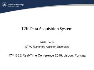
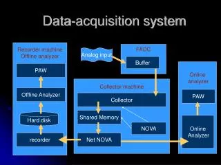
Update on the Data Acquisition System development in the UK. Valeria Bartsch, on behalf of CALICE-UK Collaboration. Host PC. Host PC. ODR. ODR. PCIe. PCIe. DIF. DIF. DIF. DIF. Detector Unit. Detector Unit. Detector Unit. Detector Unit. DAQ architecture.

E N D
Update on the Data Acquisition System development in the UK Valeria Bartsch, on behalf of CALICE-UK Collaboration
Host PC Host PC ODR ODR PCIe PCIe DIF DIF DIF DIF Detector Unit Detector Unit Detector Unit Detector Unit DAQ architecture Detector Unit:Sensors & ASICs DIF: Detector InterFace - connects generic DAQ and services LDA: Link/Data Aggregator – fanout/in DIFs & drive link to ODR ODR: Off Detector Receiver – PC interface for system. C&C: Clock & Control: Fanout to ODRs (or LDAs) 50-150 Mbps HDMI cabling 1-3Gb Fibre LDA C&C Counting Room Detector Storage LDA 10-100m 0.1-1m
Host PC Host PC ODR ODR PCIe PCIe DIF DIF DIF DIF Detector Unit Detector Unit Detector Unit Detector Unit DAQ architecture 50-150 Mbps HDMI cabling 1-3Gb Fibre LDA C&C Counting Room Detector Storage LDA 10-100m 0.1-1m
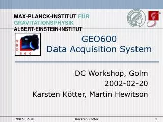
Off Detector Receiver (ODR) • Receives module data from LDA • PCI-Express card, hosted in PC. • 1-4 links/card (or more), 1-2 cards/PC • Buffers and transfers to store as fast as possible • Sends controls and config to LDA for distribution to DIFs • Performance studies & optimisation on-going Expansion (e.g. 3xSFP) Hardware: • Using commercial FPGA dev-board: • PLDA XPressFX100 • Xilinx Virtex 4, 8xPCIe, 2x SFP (3 more with expansion board) SFPs for optic link B.G., A.M @ RHUL
ODR - data access rate • transfer of the data from ODR memory to the user-program memory • => 220-320MByte/sec B.G., A.M @ RHUL
Host PC Host PC ODR ODR PCIe PCIe DIF DIF DIF DIF Detector Unit Detector Unit Detector Unit Detector Unit DAQ architecture 50-150 Mbps HDMI cabling 1-3Gb Fibre LDA C&C Counting Room Detector Storage LDA 10-100m 0.1-1m
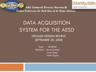
S F P S F P 10 HDMI Spartan3 FPGA USB Link Data Aggregator (LDA) • Hardware: • PCBs designed and get customized in 1week time by Enterpoint • Carrier BD2 board likely to be constrained to at least a Spartan3 2000 model • Gigabit links as shown below, 1 Ethernet and a TI TLK chipset • USB used as a testbench interface when debugging M.K., Manchester
Link Data Aggregator (LDA) Firmware: • Ethernet interface based on Xilinx IP cores • DIF interface based on custom SERDES with state machines for link control. Self contained, with a design for the DIF partner SERDES as well • Possible to reuse parts from previous Virtex4 network tests • No work done on TLK interface as of yet 1 LDA can serve 10 DIFS M.K., Manchester
Host PC Host PC ODR ODR PCIe PCIe DIF DIF DIF DIF Detector Unit Detector Unit Detector Unit Detector Unit DAQ architecture 50-150 Mbps HDMI cabling 1-3Gb Fibre LDA C&C Counting Room Detector Storage LDA 10-100m 0.1-1m
Clock and Control board • provides an input line to an external clock and an internal clock for testing and debugging • provides input lines for controls and fast trigger board to be built at RAL design finalised
Host PC Host PC ODR ODR PCIe PCIe DIF DIF DIF DIF Detector Unit Detector Unit Detector Unit Detector Unit DAQ architecture 50-150 Mbps HDMI cabling 1-3Gb Fibre LDA C&C Counting Room Detector Storage LDA 10-100m 0.1-1m
Detector Interface (DIF) status • keep DIF simple hence predictable (no local ‘memory management’, for example) • DIF proto: large Xilinx FPGA, to be slimmed down for final DIF • design ‘frozen’ (but not too cold), board layout well under way M.G, B.H, Cambridge
DIF ASU[0] ECAL slab interconnect • geometry investigated (multi-rows preferred) • technology: conductive adhesive vs. flat flexible cable (FFC), with preference to FFC • soldering technologies are being investigated (Hot-Bar soldering, laser soldering, IR soldering) M.G, B.H, Cambridge
DAQ software • Chose DOOCS framework • Ens naming service: • Facility (F), device (D), location (L), property (P) • e.g. CALICE,ODR,ODR1,LDAX • Overview over infrastructure to be build: • starting point: ODR interface • event builder needs to • be modified Disk Cache Copy Event Builder Run Controller DAQ FSM Slow Collector Fast Collector ODR1 ODR2 ODRN …. T.W. RHUL, V.B. UCL
Single Event Upset (SEU) Study finalised, submitted to NIM • SEU cross section depending on • FPGA type • traversing particle (n,p,p) • energy of traversing particle • => need to study particle spectra V.B, M.W. UCL
Single Event Upset (SEU) Study Main backgrounds: (tt, WW and bhabha scattering also studied) gg(from beamstrahlung) -> hadrons QCD events • SEU rate of 14 min-12hours depending on FPGA type for the whole ECAL, needs to be taken into account in control software • fluence of 2*106/cm per year, not critical • radiation of 0.16Rad/year, not critical • occupancy of 0.003/bunch train (not including noise) V.B, M.W. UCL
outlook • EUDET module: • DAQtest 2008: ‘minimal DIF’ hardware & firmware • EUDET beam test 2009 • Question to the detector people: • how many ODRs do we need? • how many LDAs do we need?
DIF Links Detail DIF Link DIF Link DIF Link DIF Link DIF Link Data Paths (TX and RX) Register Block Register IO
Ethernet Link Detail TBI PHY Xilinx 1000Base-X PCS IPCore Xilinx GMAC IPCore Control Block Control IO Data Paths (TX and RX)
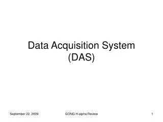
FPGA TLK serdes FPGA FPGA SFP SFP FPGA LDA DIF ODR