Download
1 / 24
240 likes | 390 Views
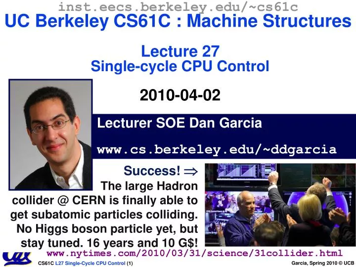
inst.eecs.berkeley.edu/~cs61c UC Berkeley CS61C : Machine Structures Lecture 27 Single-cycle CPU Control 2010-04-02. Lecturer SOE Dan Garcia www.cs.berkeley.edu/~ddgarcia.

E N D
inst.eecs.berkeley.edu/~cs61cUC BerkeleyCS61C : Machine StructuresLecture 27Single-cycle CPU Control2010-04-02 Lecturer SOE Dan Garcia www.cs.berkeley.edu/~ddgarcia Success! The large Hadroncollider @ CERN is finally able to get subatomic particles colliding. No Higgs boson particle yet, but stay tuned. 16 years and 10 G$! www.nytimes.com/2010/03/31/science/31collider.html
Instruction<31:0> instr fetch unit nPC_sel <0:15> <21:25> <16:20> <11:15> clk Rs Rt Rd Imm16 1 0 = ALU 0 0 WrEn Adr 1 1 Extender Data Memory Review: A Single Cycle Datapath • We have everything except control signals RegDst Rd Rt ALUctr MemtoReg RegWr Rs Rt zero MemWr 5 5 5 busA 32 Rw Ra Rb busW 32 RegFile busB 32 32 clk 32 imm16 Data In 16 32 clk ExtOp ALUSrc
00 PC Recap: Meaning of the Control Signals • nPC_sel: “+4” 0 PC <– PC + 4 “br” 1 PC <– PC + 4 + {SignExt(Im16) , 00 } • Later in lecture: higher-level connection between mux and branch condition “n”=next Inst Address nPC_sel 4 Adder 0 Mux 1 Adder clk PC Ext imm16
1 0 ALU 0 1 Recap: Meaning of the Control Signals • MemWr: 1 write memory • MemtoReg: 0 ALU; 1 Mem • RegDst: 0 “rt”; 1 “rd” • RegWr: 1 write register • ExtOp: “zero”, “sign” • ALUsrc: 0 regB; 1 immed • ALUctr: “ADD”, “SUB”, “OR” MemtoReg ALUctr RegDst Rd Rt MemWr RegWr Rs Rt 5 5 5 busA 32 Rw Ra Rb busW 32 RegFile busB 32 0 32 clk 32 WrEn Adr imm16 Data In 1 Extender Data Memory 16 32 clk ALUSrc ExtOp
31 26 21 16 11 6 0 op rs rt rd shamt funct 6 bits 5 bits 5 bits 5 bits 5 bits 6 bits RTL: The Add Instruction add rd, rs, rt • MEM[PC] Fetch the instruction from memory • R[rd] = R[rs] + R[rt] The actual operation • PC = PC + 4 Calculate the next instruction’s address
00 PC Instruction Fetch Unit at the Beginning of Add • Fetch the instruction from Instruction memory: Instruction = MEM[PC] • same for all instructions Inst Memory Instruction<31:0> nPC_sel Inst Address 4 Adder Mux Adder clk PC Ext imm16
31 26 21 16 11 6 0 op rs rt rd shamt funct 1 0 = ALU 0 0 WrEn Adr 1 1 Extender Data Memory The Single Cycle Datapath during Add R[rd] = R[rs] + R[rt] Instruction<31:0> instr fetch unit nPC_sel=+4 RegDst=1 <0:15> <21:25> <16:20> <11:15> clk Rd Rt Rs Rt Rd Imm16 ALUctr=ADD zero RegWr=1 Rs Rt MemtoReg=0 5 5 5 MemWr=0 busA 32 Rw Ra Rb busW 32 RegFile busB 32 32 clk 32 imm16 Data In 16 32 clk ALUSrc=0 ExtOp=x
00 PC Instruction Fetch Unit at the End of Add • PC = PC + 4 • This is the same for all instructions except: Branch and Jump Inst Memory nPC_sel=+4 Inst Address 4 Adder Mux Adder clk PC Ext imm16
31 26 21 16 0 op rs rt immediate 1 0 = ALU 0 0 WrEn Adr 1 1 Extender Data Memory Single Cycle Datapath during Or Immediate? • R[rt] = R[rs] OR ZeroExt[Imm16] Instruction<31:0> instr fetch unit nPC_sel=+4 RegDst=0 <0:15> <21:25> <16:20> <11:15> clk Rd Rt Rs Rt Rd Imm16 ALUctr=OR zero RegWr=1 Rs Rt MemtoReg=0 5 5 5 MemWr=0 busA 32 Rw Ra Rb busW 32 RegFile busB 32 32 clk 32 imm16 Data In 16 32 clk ALUSrc=1 ExtOp=zero
31 26 21 16 0 op rs rt immediate 1 0 = ALU 0 0 WrEn Adr 1 1 Extender Data Memory The Single Cycle Datapath during Load • R[rt] = Data Memory {R[rs] + SignExt[imm16]} Instruction<31:0> instr fetch unit nPC_sel=+4 RegDst=0 <0:15> <21:25> <16:20> <11:15> clk Rd Rt Rs Rt Rd Imm16 ALUctr=ADD zero RegWr=1 Rs Rt MemtoReg=1 5 5 5 MemWr=0 busA 32 Rw Ra Rb busW 32 RegFile busB 32 32 clk 32 imm16 Data In 16 32 clk ALUSrc=1 ExtOp=sign
31 26 21 16 0 op rs rt immediate 1 0 = ALU 0 0 WrEn Adr 1 1 Extender Data Memory The Single Cycle Datapath during Store • Data Memory {R[rs] + SignExt[imm16]} = R[rt] Instruction<31:0> instr fetch unit nPC_sel=+4 RegDst=x <0:15> <21:25> <16:20> <11:15> clk Rd Rt Rs Rt Rd Imm16 ALUctr=ADD zero RegWr=0 Rs Rt MemtoReg=x 5 5 5 MemWr=1 busA 32 Rw Ra Rb busW 32 RegFile busB 32 32 clk 32 imm16 Data In 16 32 clk ALUSrc=1 ExtOp=sign
31 26 21 16 0 op rs rt immediate 1 0 = ALU 0 0 WrEn Adr 1 1 Extender Data Memory The Single Cycle Datapath during Branch • if (R[rs] - R[rt] == 0) then Zero = 1 ; else Zero = 0 Instruction<31:0> instr fetch unit nPC_sel=br RegDst=x <0:15> <21:25> <16:20> <11:15> clk Rd Rt Rs Rt Rd Imm16 ALUctr=SUB zero RegWr=0 Rs Rt MemtoReg=x 5 5 5 MemWr=0 busA 32 Rw Ra Rb busW 32 RegFile busB 32 32 clk 32 imm16 Data In 16 32 clk ALUSrc=0 ExtOp=x
31 26 21 16 0 op rs rt immediate Inst Memory Adr MUX ctrl 00 PC Q: What logic gate? Instruction Fetch Unit at the End of Branch • if (Zero == 1) then PC = PC + 4 + SignExt[imm16]*4 ; else PC = PC + 4 Instruction<31:0> nPC_sel • What is encoding of nPC_sel? • Direct MUX select? • Branch inst. / not branch • Let’s pick 2nd option Zero nPC_sel 4 Adder 0 Mux 1 Adder imm16 clk PC Ext
Step 4: Given Datapath: RTL Control Instruction<31:0> Inst Memory <0:5> <21:25> <16:20> <11:15> <0:15> <26:31> Adr Op Fun Rt Rs Rd Imm16 Control ALUctr MemWr MemtoReg ALUSrc RegWr RegDst ExtOp nPC_sel DATA PATH
A Summary of the Control Signals (1/2) inst Register Transfer add R[rd] R[rs] + R[rt]; PC PC + 4 ALUsrc = RegB, ALUctr = “ADD”, RegDst = rd, RegWr, nPC_sel = “+4” sub R[rd] R[rs] – R[rt]; PC PC + 4 ALUsrc = RegB, ALUctr = “SUB”, RegDst = rd, RegWr, nPC_sel = “+4” ori R[rt] R[rs] + zero_ext(Imm16); PC PC + 4 ALUsrc = Im, Extop = “Z”,ALUctr = “OR”, RegDst = rt,RegWr, nPC_sel =“+4” lw R[rt] MEM[ R[rs] + sign_ext(Imm16)]; PC PC + 4 ALUsrc = Im, Extop = “sn”, ALUctr = “ADD”, MemtoReg, RegDst = rt, RegWr, nPC_sel = “+4” sw MEM[ R[rs] + sign_ext(Imm16)] R[rs]; PC PC + 4 ALUsrc = Im, Extop = “sn”, ALUctr = “ADD”, MemWr, nPC_sel = “+4” beq if ( R[rs] == R[rt] ) then PC PC + sign_ext(Imm16)] || 00 else PC PC + 4 nPC_sel = “br”, ALUctr = “SUB”
add sub ori lw sw beq jump RegDst 1 1 0 0 x x x ALUSrc 0 0 1 1 1 0 x MemtoReg 0 0 0 1 x x x RegWrite 1 1 1 1 0 0 0 MemWrite 0 0 0 0 1 0 0 nPCsel 0 0 0 0 0 1 ? Jump 0 0 0 0 0 0 1 ExtOp x x 0 1 1 x x ALUctr<2:0> Add Subtract Or Add Add x Subtract 31 26 21 16 11 6 0 R-type op rs rt rd shamt funct add, sub immediate I-type op rs rt ori, lw, sw, beq J-type op target address jump A Summary of the Control Signals (2/2) See func 10 0000 10 0010 We Don’t Care :-) Appendix A op 00 0000 00 0000 00 1101 10 0011 10 1011 00 0100 00 0010
Boolean Expressions for Controller RegDst = add + subALUSrc = ori + lw + swMemtoReg = lwRegWrite = add + sub + ori + lw MemWrite = swnPCsel = beqJump = jump ExtOp = lw + swALUctr[0] = sub + beq (assume ALUctr is 00 ADD, 01: SUB, 10: OR)ALUctr[1] = or where, rtype = ~op5 ~op4 ~op3 ~op2 ~op1 ~op0, ori = ~op5 ~op4 op3 op2 ~op1 op0lw = op5 ~op4 ~op3 ~op2 op1 op0sw = op5 ~op4 op3 ~op2 op1 op0beq = ~op5 ~op4 ~op3 op2 ~op1 ~op0jump = ~op5 ~op4 ~op3 ~op2 op1 ~op0 add = rtype func5 ~func4 ~func3 ~func2 ~func1 ~func0sub = rtype func5 ~func4 ~func3 ~func2 func1 ~func0 How do we implement this in gates?
Controller Implementation opcode func RegDst add ALUSrc sub MemtoReg ori RegWrite “OR” logic “AND” logic MemWrite lw nPCsel sw Jump beq ExtOp jump ALUctr[0] ALUctr[1]
Instruction<31:0> nPC_sel Instruction Fetch Unit Rd Rt <0:15> <16:20> <11:15> <21:25> Clk RegDst 1 0 Mux Rt Rs Rd Imm16 Rs Rt RegWr ALUctr Zero 5 5 5 MemWr MemtoReg busA Rw Ra Rb busW 32 32 32-bit Registers 0 ALU 32 busB 32 0 Clk 32 Mux Mux 32 1 WrEn Adr 1 Data In 32 Data Memory Extender imm16 32 16 Clk ALUSrc ExtOp Peer Instruction • MemToReg=‘x’ & ALUctr=‘sub’. SUB or BEQ? • ALUctr=‘add’. Which 1 signal is different for all 3 of: ADD, LW, & SW? RegDst or ExtOp? 12 a) SR b) SE c) BR d) BE
Summary: Single-cycle Processor • 5 steps to design a processor • 1. Analyze instruction set datapath requirements • 2. Select set of datapath components & establish clock methodology • 3. Assemble datapath meeting the requirements • 4. Analyze implementation of each instruction to determine setting of control points that effects the register transfer. • 5. Assemble the control logic • Formulate Logic Equations • Design Circuits Processor Input Control Memory Datapath Output
31 26 25 0 J-type jump op target address The Single Cycle Datapath during Jump • New PC = { PC[31..28], target address, 00 } Instruction<31:0> Jump= Instruction Fetch Unit nPC_sel= Rd Rt <0:15> <0:25> <21:25> <16:20> <11:15> Clk RegDst = 1 0 Mux Rt Rs Rd Imm16 TA26 ALUctr = Rs Rt RegWr = MemtoReg = 5 5 5 busA Zero MemWr = Rw Ra Rb busW 32 32 32-bit Registers 0 ALU 32 busB 32 0 Clk Mux 32 Mux 32 1 WrEn Adr 1 Data In 32 Data Memory Extender imm16 32 16 Clk ALUSrc = ExtOp =
31 26 25 0 J-type jump op target address The Single Cycle Datapath during Jump • New PC = { PC[31..28], target address, 00 } Instruction<31:0> Jump=1 Instruction Fetch Unit nPC_sel=? Rd Rt <0:15> <0:25> <21:25> <16:20> <11:15> Clk RegDst = x 1 0 Mux Rt Rs Rd Imm16 TA26 ALUctr =x Rs Rt RegWr = 0 MemtoReg = x 5 5 5 busA Zero MemWr = 0 Rw Ra Rb busW 32 32 32-bit Registers 0 ALU 32 busB 32 0 Clk Mux 32 Mux 32 1 WrEn Adr 1 Data In 32 Data Memory Extender imm16 32 16 Clk ALUSrc = x ExtOp = x
31 26 25 0 J-type jump Inst Memory Adr Adder Mux Adder op target address Instruction Fetch Unit at the End of Jump • New PC = { PC[31..28], target address, 00 } Jump Instruction<31:0> nPC_sel Zero nPC_MUX_sel How do we modify thisto account for jumps? 4 00 0 PC 1 Clk imm16
31 26 25 0 J-type jump Inst Memory Adr Adder Mux Mux Adder op target address Instruction Fetch Unit at the End of Jump • New PC = { PC[31..28], target address, 00 } Jump Instruction<31:0> nPC_sel Zero • Query • Can Zero still get asserted? • Does nPC_sel need to be 0? • If not, what? nPC_MUX_sel 26 00 4 00 1 TA PC 0 4 (MSBs) 0 Clk 1 imm16