Download
1 / 28
280 likes | 555 Views
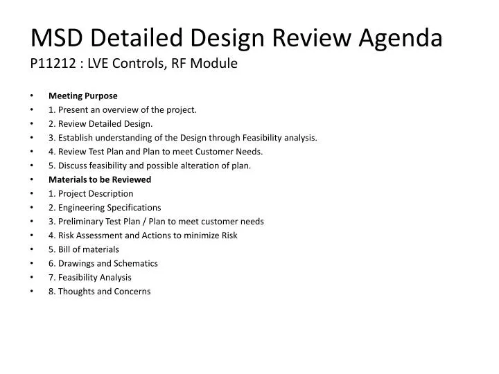
MSD Detailed Design Review Agenda P11212 : LVE Controls, RF Module. Meeting Purpose 1. Present an overview of the project. 2. Review Detailed Design. 3. Establish understanding of the Design through Feasibility analysis. 4 . Review Test Plan and Plan to meet Customer Needs.

E N D
MSD Detailed Design Review AgendaP11212 : LVE Controls, RF Module • Meeting Purpose • 1. Present an overview of the project. • 2. Review Detailed Design. • 3. Establish understanding of the Design through Feasibility analysis. • 4. Review Test Plan and Plan to meet Customer Needs. • 5. Discuss feasibility and possible alteration of plan. • Materials to be Reviewed • 1. Project Description • 2. Engineering Specifications • 3. Preliminary Test Plan / Plan to meet customer needs • 4. Risk Assessment and Actions to minimize Risk • 5. Bill of materials • 6. Drawings and Schematics • 7. FeasibilityAnalysis • 8. Thoughts and Concerns
GUI Mockups • GUI mockups are images meant to get the idea of the GUI, rather than a working implementation • The following windows have been mocked up: • The Main window • The Main window’s menu bar • The joystick configuration screen • The keyboard configuration screen
System Analysis • Delay through transmission: • Theoretical message size: 18 bits • Single Message Latency: • Time through USART: 18b / 31kBps = 72us • Time through RF: 18b / 40kbps = 450us • Total time: 72us + 450us = 522us • Max messages: 5 • Max messages size: 90 bits • Max Message Latency: • Time through USART: 90b / 31kBps = 362us • Time through RF: 90b / 40kbps = 2.2ms • Total time: 362us + 2200us = 2.562ms • Forward Backward Left Right M1 + M1 - M2 + M2 - M3 + M3 - M4 + M4 - M5 + M5 - M6 + M6 - M7 + M7 - M8 + M8 – • 5 bit: instruction 0-31 • 4 bit: speed 0-15 • X bit: redundancy • 5 instructions at once • (5+4+9)*5= 90 bits/instruction set
System Analysis • VIN = 7.2v • IOUT(max)= 3.3A per motor • Absolute Max ratings • VSS=50v • IO • Peak non-repetitive = 3A • Repetitive = 2.5A • DC operation = 2A • PTotal= Total power Dissipation at 75C is 25W • Operating temperature -25C to 130C • As you can see the Peak non-repetitive is below the possible IOUT so an alternative configuration is required. From the L298 data sheet found at http://www.st.com/stonline/books/pdf/docs/1773.pdf • Using a Paralleled input and output configuration the L298 can support up to 3.5A of repetitive peak current. • Design will require 1 L298 in a paralleled configuration per motor. • PTotal >= VIN*IMAX 25 > 23.76 • VIN<= VSS MAX
System Analysis • VLOGIC from Nano dev board is 5V which falls within the acceptable range. • IIH from Nano dev board is 40μA which is less than 100μA • Requirements for ArdunioNano • Input Voltage 6-20V, 7.2 falls in the range • Current draw on the Nano Dev board • L298 72mA • Atmega 12mA • L298ENABLE 2mA • FTDI 15mA • LEDs 5mA • Total draw = 116mA • Total supported 500mA
System Analysis • Based on previous years thermal considerations the primary concern for heat generation in the design was the voltage regulation. Because our current design does not have a voltage regulator besides the one on the Micro-Controller dev board it will not have to be considered. The next board component of concern was the H-bridge for this the following equations will be used • Δt = PDMAX * Rjc and Tjmax = Δt + Tamb • PDMAX=25W • Rjc= 3C/W • Δt=75C • Tjmax = 75+22=97C • This value is within the effective operating range of -25 to 130C.