Download
1 / 16
210 likes | 433 Views
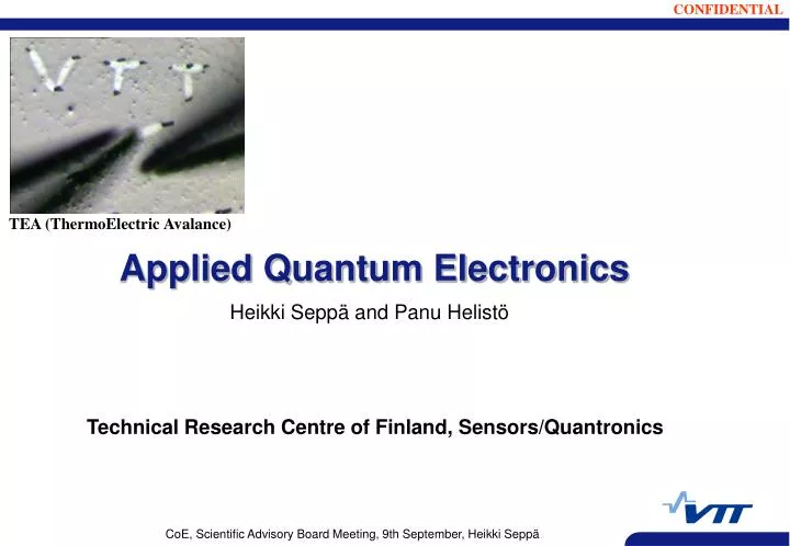
Applied Quantum Electronics. TEA (ThermoElectric Avalance). Heikki Seppä and Panu Helistö. Technical Research Centre of Finland, Sensors/Quantronics. Motivation - Proactive Inventions and Innovations. Facts. Virtual needs. Real needs. Future real needs. Visions and imagination.

E N D
Applied Quantum Electronics TEA (ThermoElectric Avalance) Heikki Seppä and Panu Helistö Technical Research Centre of Finland, Sensors/Quantronics
Motivation - Proactive Inventions and Innovations Facts Virtual needs Real needs Future real needs Visions and imagination Research Centres Univeristies Enterprises BasicResearch AppliedResearch Development Needs andCustomers Future Needs andCustomers Innovations Proactive Innovations
Contents • Research Examples (2006) • Towards quantum computer • Teraherts imaging • Invisible printable electric codes, carbon nanotubes • Thermoelectric avalance in metalic nano arrays • Recent projects and submitted project applications • Patent applications (2006) • Other results • Future plans
Maria Gabriella Castellano, Leif Grönberg, Pasquale Carelli, Fabio Chiarello, Carlo Cosmelli, Roberto Leoni, Stefano Poletto, Guido Torrioli, Juha Hassel, Panu Helistö, Superconducting Science and Technology 19, 860864 (2006). J. Hassel, H. Seppä, P. Helistö, J. Kunert, L. Fritzsch and H.G. Meyer, Appl. Phys. Lett., accepted (2006) Towards quantum computing with superconducting solid state qubits • Main problem: decoherence due to thermal noise and fluctuators in junctions and their neighborhood • RSFQubit results 2006 • high quality JJ junctions => reduced JJ noise • e-ph coupling 'cooling fins' to achieve record low base temperature of shunt resistors • RC shunts to isolate qubit from RSFQ dissipations • Decoherence times ~5 us achieved
Background (reflected by concealed objects) at room temperature Skin at body temperature Passive imaging with superconducting bolometers NIST - VTT collaboration • 1-pixel Nb bolometer 0.1 - 1 THz • RT readout • Linear scanning • (2005)
NbN bolometer arrays fabricated at VTT P. Helistö, A. Luukanen, L. Grönberg, J.S. Penttilä, H. Seppä, H. Sipola, C.R. Dietlein and E.N. Grossman, Antenna-coupled microbolometers for passive THz direct detection imaging arrays, 36th European Microwave Conference 2006, Manchester 1015 September 2006 . • NbN - higher normal state resistance=> lower thermal conductance than Nb (lower noise), easier matching to antenna • Tc can be tailored to optimize performance 0 - 13 K • 8-pixel subarrays developed => goal 128-pixel linear array
The VTT room-temperature readout • A novel readout method developed by VTT utilizes ETF • Simple low noise JFET amplifier reads out the voltage across the bolometer • With feedback through Zfb, voltage across bolometer is set to V • At high frequencies, Zx maintains stability • Bias point set at the bottom of the IV curve large Rd allows for easy noise matching • H Seppä and P Helistö, pat. pend.
Electrical noise of a NbN microbolometer + RT readout J.S. Penttilä, A. Luukanen, L. Grönberg, P. Helistö, H. Sipola, and H. Seppä, Seventh International Workshop on Low Temperature Electronics, WOLTE 7, WPP264, 2123 June 2006, ESTEC, Noordwijk, The Netherlands, 203207 (2006). • First run of NbN test detectors • Smooth IV curve - good quality bolometer wire • Electrical NEP ~ 9 fW/sqHz (lowest measured at 4 K) NEP (fW/rtHz) 2 4 6 8 10 V [mV]
Sheet resistance at 10 kHz 230306NC 2,93 μm 630 Ω/□ 354 Ω/□ 020306Ag 500 nm 4,93 Ω/□ 695 Ω/□ 210306NC 35 nm 18,1 k Ω/□ 3,79 kΩ/□ 210306NC2 24 nm 103,4 k Ω/□ 32,7 k Ω/□ Printable nanotube based invisible electric code • Utilizes proberties of single walled proberties nanotubes • Near completely invisible • Sufficient condactivity to electric detection (100 MHz) • Applications: • Invisible electric codes • Printable active components
Nanoparticle TEM visualization thin polymer shell ~ 5 Å time
Electric Sintering Condactivity via tunneling (inelastic or elastic cotunneling ?), strong temperature dependence SEM before electrical sintering Room temperature sintering process Metallic coductivity SEM after electrical sintering
Thermoelectric Avalance AFM 100 mm Click Video melted wire self-organized creation of sintered or melted metallic wire - uniform width, - large aspect ratio SEM not sintered nanoparticle array 100 mm
Projects Quantronix (Panu Helistö) • Submm Scanner, Tekes, Companies, (NIST), 2005 - 2007 • Printag, Tekes/FinNano, Companies, 2005 - 2007 • RSFQubit, EU FP6, 2005 - 2007 • Low-temperature Spectrometer Array, ESA GSTP G204-06M (SRON, 2007-2008) • Superconducting Read Out for Microcalorimeters, ESA TRP SCI-X10.a (SRON, 2007-2008) • Quantum Metrology Rriangle, Technology Industries of Finland, (MIKES, TKK, 2007-2010). • TeraEye, EU FP6, THz imaging based on quantum dot detectors, in negotiation, 2007 - 2009 • ITI, Thermoplexer, submitted (ESA) Printable Sensors (Ari Alastalo) • Printable Electronics …, VTT, 2005 - • Printed RFID Sensor Solutions, Nordite/Tekes, 2006 - 2007 • Printable Functional Nano Structures, submitted to Teknologiateollisuuden säätiölle, 2007 - 2009 • Metallic and semiconducting nanoparticles for printable electronics, planning phase, EU-7 Biosensors (Kirsti Tappura) • Biosystems, VTT, 2005 - • MEMS Based Later Bulk Acoustic Waves for Biosensors, Tekes, Companies, (2005 - • MEMS based Biosensors, planning phase, EU7, 2007 -2010 • Terahertz Biospectrometer, planning phase, EU7, 2007 - 2010
Recent Patent Applications • Directly linked to CeO • Bolometer Amplifier based on the Thermoelectric Feedback, 2006 • Multiplexing Scheme based on Thermoelectric Power Amplification and SIN-Junctions, 2006 • Invisible Ink for Electric Coding based on Carbon Nanotubes, 2006 • Sintering of Nanoparticles using Thermoelectric Avalance, 2006 • Indirectly linked to CeO • Several patent applications (2006, about 15) related to sensors, materials, telecommunication, • 5 - 6 patents are lisenced or sold during 2006
Other Results • New Research Team (Dr. Ari Alastalo) • Two Doctoral Thesis: Ari Alastalo and Anu Kärkkäinen • Two Spin-off Companies and one Join Company Directly Related to CeO • Aivon Ltd, 2006, cryogenic detectors, dc and hg SQUIDs for Electa- Neuromag, Dr. Jari Penttilä (Shares: three Finns and VTT) Indirectly Related to CeO • FennoID Ltd, 2006, RFID sollutions, Heikki Mamia (Shares: two Finns, German, Chinese, Indonesian and VTT) • ReadTeck (Chína), 2006, Joint Company between FennoID (Finland) and TeckTop (China/Wuhan), RFID for China Markets (Traffic Customs) and Electric Codes
Future Plans • Directly Related to CeO • Teraherts Imiging Systems • Teraherts Spectroscopy • New Realisation for Quantum Triangle • Sluice, BOT, unSQUID / Calorimetric detection of electrons • Detectors and Electronics for Quantum Computing • RFSQ • Modified un SQUID (Quantum Limited Amplifier) • Prediction: 12 times lower energy resolution than dc SQUID • Indirectly Related to CeO • Electric conductivity in 3D nano arrays • Inorganic nanoparticles (metalic, semiconductive and ferroelectric) for printable electronics • Terahertz spectroscopy for biotechnolgy