Download
1 / 24
290 likes | 545 Views
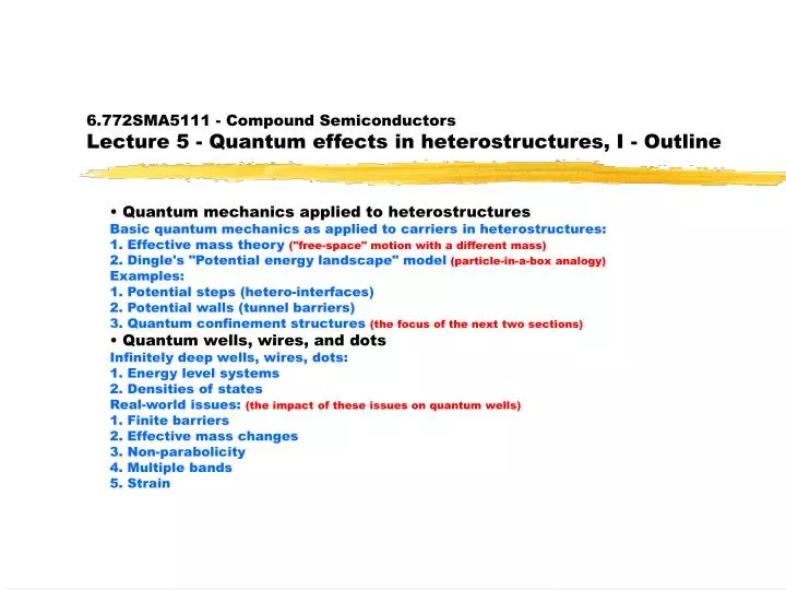
6.772SMA5111 - Compound Semiconductors Lecture 5 - Quantum effects in heterostructures, I - Outline. • Quantum mechanics applied to heterostructures Basic quantum mechanics as applied to carriers in heterostructures: 1. Effective mass theory ("free-space" motion with a different mass)

E N D
6.772SMA5111 - Compound SemiconductorsLecture 5 - Quantum effects in heterostructures, I - Outline • Quantum mechanics applied to heterostructures Basic quantum mechanics as applied to carriers in heterostructures: 1. Effective mass theory ("free-space" motion with a different mass) 2. Dingle's "Potential energy landscape" model (particle-in-a-box analogy) Examples: 1. Potential steps (hetero-interfaces) 2. Potential walls (tunnel barriers) 3. Quantum confinement structures (the focus of the next two sections) • Quantum wells, wires, and dots Infinitely deep wells, wires, dots: 1. Energy level systems 2. Densities of states Real-world issues: (the impact of these issues on quantum wells) 1. Finite barriers 2. Effective mass changes 3. Non-parabolicity 4. Multiple bands 5. Strain
Quantum mechanics for heterostructuresTwo powerful, simplifying approximations • Effective Mass Theory(the most important concept in semiconductor physics) Electrons in the conduction band of a nearly perfect semiconductor lattice can be modeled as though they are moving in free space, but with a different mass (their "effective mass"). Their wavefuction, y(x), satisfies the Schrodinger Equation with an appropriate mass and potential energy function: –(-h2/2m*)∂2Ψ(x)/∂x2 = [E - V(x)] Ψ(x) Similarly, empty valence bonds can be modeled as positively charged particles (holes) moving in free space with their own effective mass. • Potential energy landscape model(Ray Dingle, et al, ca. 1974) In heterojunctions electrons and holes can be modeled by the effective mass theory, even though perfect periodicity is destroyed. In this case, the potential energy profile, V(x), seen by electrons is Ec(x) and that seen by holes is Ev(x).
Quantum mechanics, cont. Schrodinger Equation in three dimensions: (-ћ2/2m*)[∂2/∂x2 +∂2/∂y2 +∂2/∂z2] Ψ(x,y,z) = [Ex + Ey + Ez - V(x,y,z)] Ψ(x,y,z) Corresponding wave function: Ψ(x,y,z) = Ψx(x) Ψy(y) Ψz(z) Where V is a constant, the solutions are (1) Plane waves if E > V, i.e. Ψ(x,y,z) = A exp [±i(kxx + kyy + kzz)], with E - V = [Ex + Ey + Ez - V(x,y,z)] = (ћ2 /2m*)(kx 2 + ky2 + kz2) (2) Decaying exponentials if E < V, i.e. Ψ(x,y,z) = A exp -(kxx + kyy + kzz), with V - E = [V - Ex - Ey - Ez] = (ћ2 /2m*)(kx 2 + ky2 + kz2)
Common 1-d potential energy landscapes A one-dimensional potential step: Classically, electrons with 0 < E < ΔEc cannot pass x = 0, while those with E > ΔEc do not see the step. Quantum mechanically, electrons with 0 < E < ΔEc penetrate the barrier with an exponential tail, and those with E > ΔEc have a finite probability of being reflected by the step.
Common 1-d potential energy landscapes, cont. A one-dimensional potential barrier (tunnel barrier): Classically, electrons with 0 < E < ΔEc can again not pass x = 0, while those with E > ΔEc do not see the barrier at all. Quantum mechanically, electrons with 0 < E < ΔEc can penetrate the barrier and some fraction can pass right through it, i.e. "tunnel," while a of fraction of those with E > ΔEc will be reflected by the step.
Quantum Tunneling through Single Barriers Transmission probabilities - Ref: Jaspirit Singh, Semiconductor Devices - an introduction, Chap. 1 Rectangular barrier
Common 1-d potential energy landscapes, cont. A one-dimensional resonant tunneling barrier: Classically, electrons with 0 < E < ΔEc can again not pass from one side to the other, while those with E > ΔEc do not see the barriers at all. Quantum mechanically, electrons with 0 < E < ΔEc with energies that equal energy levels of the quantum well can pass through the structure unattenuated; while a fraction of those with E > ΔEc will be reflected by the steps.
Common 1-d potential energy landscapes, cont. A one-dimensional potential well: Classically,electrons with 0 < E < ΔEc are confined to the well, while those with E > ΔEc do not see the well at all. Quantum mechanically,electrons can only have certain discrete values of 0 < E < ΔEc and have exponential tails extending into the barriers, while a fraction of those with E > ΔEc have a higher probability of being found over the well than elsewhere.
Three-dimensional quantum heterostructures- quantum wells, wires, and dots The quantities of interest to us are 1. The wave function 2. The energy levels 3. The density of states: As a point for comparison we recall the expressions for these quantities for carriers moving in bulk material: Wave function: Ψ(x,y,z) = A exp [±i(kxx + kyy + kzz)] Energy: E - Ec = (ћ2/2m*)(kx2 + ky2 + kz2) Density of states:ρ (E) = (1/2π2) (2m*/ћ)3/2 (E - Ec)1/2
Three-dimensional quantum heterostructures- quantum wells, wires, and dots The 3-d quantum well: In an infinitely deep well, i.e. ∆Ec = ∞, dx wide: Wave function: Ψ(x,y,z) = An sin (nπx/dx) exp [±i(kyy + kzz)] for 0 ≤ x ≤ dx = 0 outside well Energy: E -Ec = En + (ћ2/2m*)(ky2 + kz 2) 2 with En = π2h2n2/2m*dx2 Density of states:ρ(E) = (m*/π2ћ) for E ≥ En for each n
Three-dimensional quantum heterostructures- quantum wells, wires, and dots In an infinitely deep wire, i.e. ∆Ec = ∞, dx by dy: Wave function: Ψ(x,y,z) = Anm sin (nπx/dx) sin (mπx/dy) exp [±i kzz)] for 0 ≤ x ≤ dx, 0 ≤ y ≤ dy = 0 outside wire Energy: E -Ec = En,m + (ћ2/2m*) kz2 with En,m = (π2ћ2 /2m*)(n2/dx2 + m2/dy2) Density of states:ρ(E) = {m*/[2ћ2 π2(E - Ec - En,m)]}1/2 for each n,m Note: some combinations of n and m may give the same energies
Quantum Wells, Wires, Boxes: Density of States The 3-d quantum box: In an infinitely deep box, i.e. ∆Ec = ∞, dx by dy by dz: Wave function: Ψ(x,y,z) = Anm sin (nπx/dx) sin (mπx/dy) sin (pπx/dz) for 0 ≤ x ≤ dx, 0 ≤ y ≤ dy , 0 ≤ z ≤ dz = 0 outside box Energy: E - Ec = En,m,p Density of states: ρ(E) = one per box for each combination of n, m, and p Note: some combinations of n and m may give the same energies
Three-dimensional quantum heterostructures- quantum wells, wires, and dots 1. Bulk material Volume in k-space per state: Volume in k-space occupied by states with energy less than E: Number of electron states in this volume: Density of states with energies between E and E+dE per unit volume:
Quantum Wells, Wires, Boxes: Density of States 2. Quantum well Area in 2-d k-space (i.e., ky,kz) per state: Area in k-space occupied by staes with energy less than En: Number of electrons in this area in band n: Density of states in well band n between E and E+dE per unit
Quantum Wells, Wires, Boxes: Density of States 3. Quantum wire Distance in k-space per state: 2 π/ L Distance in k-space occupied by states with energy less than En,m: Number of electron states in this length in band n,m: Density of states in wire band n,m between E and E+dE per unit wire
Quantum Wells, Wires, Boxes: Density of States 4. Quantum box In this situation the density of states is simply the number of states per box, which is 2, at each possible discrete energy level,, E n,m p, times the degeneracy of that energy level, i.e, the number of combinations of n, m, and p that result in the same value of E n,m p.
Additional issues with wells - extensions to wires and boxesfollow same arguments Real world issues: finite barriers heights: wavefunctions now penetrate into barriers and treatment is algebraically more complicated, but straightforward. Wavefunction and its derivative must be continuous. m* discontinuities: if masses in well and barriers differ this must be taken into account when matching wavefunction at boundaries non-parabolicity: if effective mass changes with energy the correct value of m* must be used. This usually requires iteration of the solutions, another annoying complication (but not hard). multiple bands: in the valence band there are typically two hole bands (light and heavy) that must be considered and they may interact if they overlap to complicate the picture (following foils) strained wells: strain will shift the light and heavy hole bands and modify the starting point, bulk band picture (following foils)
Quantum well levels with multiple valence bands 10 nm wide wells Al0.3Ga0.7As/GaAs Al 0.3Ga0.7As/In0.1Ga0.9As
More QW levels with multiple valence bands (Image deleted) See G. Bastard and J.A. Brum, "Electronic States in Semiconductor Heterostructures," IEEE J. Quantum Electon., QE-22 (1986) 1625.
Impact of strain and QW quantization on bands 15 nm wide wells GaAs / In0.06Ga0.57Al 0.37As
Final comments - additional structures of interest Other structures triangular and parabolic wells coupled wells (next time) superlattices (next time)