Download
1 / 37
380 likes | 555 Views
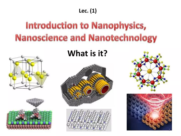
Lec . (1). Introduction to Nanophysics, Nanoscience and Nanotechnology. What is it?. What is Nanophysics, Nanoscience and Nanotechnology?. Eigler et al. NATURE 363, 1993.

E N D
Lec. (1) Introduction to Nanophysics, Nanoscience andNanotechnology • What is it?
What is Nanophysics, Nanoscience and Nanotechnology? Eigler et al. NATURE 363, 1993 Nanoscience and nanotechnology are the study and application of extremely small things and can be used across all the other science fields, such as chemistry, biology, physics, materials science, and engineering. • How is nanoscience different than • Chemistry • Biology • Physics • What distinguishes nanoscience from other sciences?
Physicist Richard Feynman Richard Feynman is the father of nanotechnology. with a talk entitled “There’s Plenty of Room at the Bottom” at an American Physical Society meeting at the California Institute of Technology (CalTech) on December 29, 1959, long before the term nanotechnology was used. Feynman described a process in which scientists would be able to manipulate and control individual atoms and molecules. Over a decade later, in his explorations of ultraprecision machining, Professor Norio Taniguchi coined the term nanotechnology. It wasn't until 1981, with the development of the scanning tunneling microscope that could "see" individual atoms, that modern nanotechnology began.
A scanning tunneling microscope (STM) is an instrument for imaging surfaces at the atomic level. Its development in 1981 earned its inventors, Gerd Binnig and Heinrich Rohrer (at IBM Zürich), the Nobel Prize in Physics in 1986 For an STM, good resolution is considered to be 0.1 nm lateral resolution and 0.01 nm depth resolution.[3] With this resolution, individual atoms within materials are routinely imaged and manipulated. The STM can be used not only in ultra-high vacuum but also in air, water, and various other liquid or gas ambients, and at temperatures ranging from near zero kelvin to a few hundred degrees Celsius.[4] The STM is based on the concept of quantum tunneling. When a conducting tip is brought very near to the surface to be examined, abias (voltage difference) applied between the two can allow electrons to tunnel through the vacuum between them. The resulting tunneling current is a function of tip position, applied voltage, and the local density of states (LDOS) of the sample.[4] Information is acquired by monitoring the current as the tip's position scans across the surface, and is usually displayed in image form.
Nanotechnology is the creation of functional materials, devices, and systems through control of matter on an atomic or molecular scale. The creation and use of structures, devices and systems that have novel properties and functions because of their small and/or intermediate size. DEFINITION OF NANOTECHNOLOGY PLAR - Nanotechnology
Nano: The Middle Ground Subatomic/Nuclear Particle Molcular/Atomic Scale ? “Nanoscopic” “Microscopic” “Macroscopic” ? ? Galactic 1020 m 1010 m 10-6 m 101 m 10-9 m 10-15 m 10-10 m
UNIQUENESS OF NANOMATERIALS Grains, pores, interface thickness and defects are of similar dimensions. Nanomaterials have a large surface area but their volume is very small. Improve mechanical properties (increased strength, toughness etc.,) High melting point compounds.
nanotechnology were developed for many current challenges facing the international community, including: • Clean, secure, affordable energy; • Stronger, lighter, more durable materials; • Low-cost filters to provide clean drinking water; • Medical devices and drugs to detect and treat diseases more effectively with fewer side effects; • Lighting that uses a fraction of the energy associated with conventional systems; • Sensors to detect and identify harmful chemical and biological agents; andTechniques to clean up harmful chemicals in the environment.
FIELDS OF NANOTECHNOLOGY Nanomedicine Nanobiotechnology Nanolithography Nanoelectronics Nanotechnology Nanomagnetics Nano Biodevices Nano Biomimetic materials NEMS (nano electro mechanical sys) Nano Pulp & Paper Technology
Applications of NanomaterialBased Products • Automotive industry • Engineering • Medicine • Cosmetics • Textile • Sports • Chemical industry • Electronic industry
Applications of Nanotechnology in industrial and technical fields: • ExxonMobil is using zeolites, minerals with pore sizes of less than 1 nm, as a more efficient catalyst to break down or crack large hydrocarbon molecules to form gasoline. • IBM has added nanoscale layering to disk drives, thus exploiting the giant magnetoresistive effect to attain highly dense data storage. • Gilead Sciences is using nanotechnology in the form of lipid spheres, also known as liposomes, which measure about 100 nm in diameter, to encase an anticancer drug to treat the AIDS-related Kaposi’s sarcoma. • Carbon Nanotechnologies, a company co-founded by buckyball discoverer Richard E. Smalley, is making carbon nanotubes more affordable by using a new and more efficient manufacturing process. • Nanophase Technologies is utilizing nanocrystalline particles, incorporated into other materials, to produce tough ceramics, transparent sun blocks, and catalysts for environmental uses, among other applications.
What is Nanotechnology? The Space Elevator? Ultra high strength materials allow tower to be built into space !(?)
What is Nanotechnology? Tiny machines in your body curing cancer?
What is Nanotechnology? DNA Computers in a beaker that vastly outperform our fastest supercomputers?
Nanotechnology APPLICATIONS Super fast/small computers Super strong materials Super Slippery Materials Tissue Engineering Drug Delivery Sensors TECHNOLOGIES Nanomaterials Nanolithography Scanning Probe Microscopy Self-Assembly
Materials Science: Nanomaterials Human Made Materials Biologically made materials
Silica Calcium Carbonate Calcium phosphate Hydroxyapatite Calcite
NANO- TEXTILE APPLICATIONS Nano Jacket Nano tie and scarf Student’s uniform
NANOTECHNOLOGY – FUEL CELL Atlantic – Aprilia fuel cell bike Photovoltaic cell Hydrogen Fuel Cell
Carbon Nanotubes CHIN WEE SHONG : AgS2 cubes National University of Singapore Department of Chemistry Quantum dots
Carbon Nanotubes Buckminster Fullerene C60 Smalley, Curl, Kroto. Nobel Prize
Diamond Buckyball Graphite Nanotube The Forms of Carbon Graphein: (Greek) to write
What’s the big deal about carbon nanotubes??? • Amazing Mechanical Properties • Amazing Electrical Properties: • Can be conductors or semiconductors • Could be the building block of nanocomputing
Applications: Composite Materials nanotubes poking out of fractured edge of polymer composite
Applications: Field Emission 1 Samsung prototype carbon nanotube display
Applications: Field Emission 2 Otto Zhou. UNC Physics Cold Cathode X-ray machine The potential advantages of the future CNT X-ray devices are fast response time, programmable xray intensity, programmable spatial distribution (Figure 3), ultra-fine focal spot, rapid pulsation capacity, long lifetime, low energy consumption, miniaturization, and low cost.
Synthesis of Nanomaterials Synthesis of Nanomaterials Top - down method (Destruction) Bottom-upmethod (Construction)
Synthesis of Nanomaterials Top - Down method High energy Ball Milling Lithography Gas condensation Severe plastic deformation
SYNTHESIS OF NANOMATERIALS Bottom Up method Physical Vapor Deposition Chemical Vapor Deposition Plasma Processes Sol-gel Processing Soft- Lithography Self- Assembly
CHARACTERIZATION AND DETECTION TECHNIQUES Essential requirements for the development, manufacturing and commercialization of nanomaterials is their physical, chemical and biological properties on a nanoscale level For determination of atomic structure and chemical composition of solid or liquid nanomaterials – spectroscopic methods, X-ray and Neutron diffraction For determination of size and shape – Electron microcopies (SEM or TEM)
HIGH DEPTH OF FIELD NANOMATERIAL Scanning Electron Microscope transmission electron microscope Optical Microscope
Photo detector Laser Beam Cantilever Tip Line Scan Surface Tip Atoms Force Surface Atoms WORKING PRINCIPLE OF AFM www.shef.ac.uk/~htsl/afm.htm Atomic Force Microscope