Download
1 / 12
120 likes | 202 Views
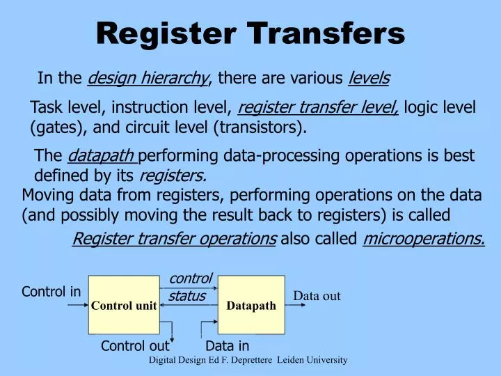
control. Data out. Control unit. Datapath. Control in. status. Control out. Data in. Register Transfers. In the design hierarchy , there are various levels. Task level, instruction level, register transfer level, logic level (gates), and circuit level (transistors).

E N D
control Data out Control unit Datapath Control in status Control out Data in Register Transfers In the design hierarchy, there are various levels Task level, instruction level, register transfer level, logic level (gates), and circuit level (transistors). The datapath performing data-processing operations is best defined by its registers. Moving data from registers, performing operations on the data (and possibly moving the result back to registers) is called Register transfer operations also called microoperations. Digital Design Ed F. Deprettere Leiden University
16 15 14 13 12 11 10 9 8 7 6 5 4 3 2 1 0 DA AA BA M FS M W B D R Control word n Register file: m m is number of address bits: 2 registers Write D data D address A address B address A data B data m m n 2 Register file m m Constant in 1 0 Mux B MB select Address out n n Data out Bus A Bus B 5 A B Function unit FS V C N Z Data in F MD select 0 1 Mux D Datapath three registers can be active at the same time: 2 (A,B) to read from, 1 (D) to write to all in one clock cycle. Buses: 2 buses, bus A and bus B, n-bit wide. Mux B selects between RF and Constant. Function unit: Contains arithmetic/logic unit (ALU) and Barrel shifter. FS is a function select code. Status bits are Z (1 if result is all 0), N (sign) C (carry) and V (overflow). Digital Design Ed F. Deprettere Leiden University
15 0 15 8 7 0 R1 PC(L) PC(H) t : B goes high t+1: transfer occurs B B: R1(7:0) R2(7:0), R2(7:0) R1(7:0), R3 M[R4] B Load R2 R1 n Boolean condition Transfer if B = 1 Simultaneously Memory to register Memory address in R4 Other example: ( if-then-else) B1: R0 R1, B1B2: R0 R2 Registers R and PC are names of registers. (or PC(15:8) and PC(7:0) Transfer operations: Digital Design Ed F. Deprettere Leiden University
n load enable n Write D data D address A address B address A data B data m 2 Mux B m decoder n 2 Register file R0 m m decoder Mux A 2 2 Load R Load Enable Bus n R0 R2 R1 n R0 R1 R2 R1 Bus MUX Select Load Enable Register File & Bus Register transfer here is multiplexer based. Bus based is another possibility: Digital Design Ed F. Deprettere Leiden University
Address Decoder Data bus destination decoder Timing/control Enable Data bus source decoder R1 A0 A1 A2 Enable Load R1 D0 D1 D2 Address bus k Data bus n Read Write k 2 n memory Read: Dx M[Ax] Write: M[Ax] Dx Examble: Memory transfer Digital Design Ed F. Deprettere Leiden University
5 A B Function unit FS V C N Z H select G select 5 B A B ALU Shifter F S S2:0 || Cin 4 2 0 0 IR IL H G Zero Detect A n-bit G MF select Mux F B parallel adder S0 S1 Cout Cin F : A, A, B, A+1, A-1, A+B A+B, A+B+1, A+B+1. MF=0, Arithm. MF=0, Logic 0 = ALU 1 = Shifter Gselect MF=1 Hselect Function unit Consists of an ALU and a Shifter. Suppose ALU is: Micro operations: F FS = MFselect S2 S1 S0 Cin F : AB, AB, AB. F : srB, slB Digital Design Ed F. Deprettere Leiden University
With Shifter words can be shifted right or left , over one or more bits: . Alternative: combinational circuit: . B0 IR IL 0 1 2 m u x 0 1 2 m u x 0 1 2 m u x 0 1 2 m u x S S S S 2 H0 Barrel Shifter is similar (bit more involved) but allows to shift over more than one bit (2 m >0 or m<0) m Moving in a 0 at the most or least significant bit position or rotated: Entering outgoing bits at the other side (wrap around) The bidirectional shiftregister with parallel load could be used. Cost: three clock pulses (load into SR, shift, transfer to R) Digital Design Ed F. Deprettere Leiden University
RTL symbolics Meaning R0 R1 + R2 contents of R1 plus R2 transferred to R0 R2 R2 1’s complement of content of R2 R2 R2 + 1 2’s complement of content of R2 R0 R1 + R2 + 1 contents of R1 minus R2 transferred to R0 R1 R1 + 1 increment content of R1 R1 R1 – 1 decrement content of R1 R2 XB: R1 R1 + R2, XB: R1 R1 + R2 + 1 Cn-1 Adder/subtractor X (B1 + B2) : R1 R2 + R3, R4 R5 R6 Cn B R0 R1 logic NOT R0 R1 R2 logic AND R0 R1 R2 logic OR R0 R1 R2 logic XOR V C R1 R1 sl R2 shift left R1 sr R2 shift richt Micro operations Arithmetic, logic and shift micro operations. Logic plus (OR) Microoperation OR Meaning: 1’s complement, clear bits, set bits, complement bits Digital Design Ed F. Deprettere Leiden University
15 14 13 12 11 10 9 8 7 6 5 4 3 2 1 0 • DA AA BA M FS M R • B D W • R1 R2 R3 R A + B + 1 F W • 001 010 011 0 00101 0 1 Bit Field Symbolic Binary Microoperation: R1 R2 + R3 +1 Control Word encoding. Timing (simulation). Depends on the complexity of the combinational circuit parts. Assume: propagation delays of CC parts are small with respect to clock period. This means that status bits, Address out and Data out (MB = 0) change at the same time as the register values. Changes in registers as a result of a microoperation appear at the clock cycle after that in which the microoperation is specified. (positve edge triggered FFs!) Values of status bits, Address out and Data out appear in the same clock cycle. Values of Constant in and Data in are placed in the clock cycle in which they are Needed. Digital Design Ed F. Deprettere Leiden University
n 3ns 3ns 1ns 4ns 1ns Write D data D address A address B address A data B data Clock m m n 2 Operand fetch 4ns Execute 4ns Write back 4ns Total 12ns Register file m m Constant in 1 0 MB select Mux B 1ns Address out n n Bus A Bus B Data out 5 A B Function unit FS Operand fetch 4ns Execute 5ns Write back 5ns Total (say) 15ns V C N Z Data in 1ns F MD select 0 1 Mux D Pipelined Datapath Suppose datapath design leads to a maximum clock frequency of 83.3 Mhz, because: All to be done in one clock cycle of 12ns. Introduce two extra registers (pipeline registers) i.e,2 extra ns. All to be done in one clock cycle of 15ns? NO! Digital Design Ed F. Deprettere Leiden University
OF OF OF OF OF OF EX EX EX EX EX EX WB WB WB WB WB WB Microinstruction k k+1 k+2 Pipeline is filling fully utilized emptying No, Because, due to pipeline registers, we can do Write back of microinstruction k (5ns) Execute of microinstruction k + 1 (5ns) Fetch operand of microinstruction k + 2 (5ns) In the same clock period of 5 ns, which is at 200Mhz clock frequency Clock period 1 2 3 4 (k) 5 (k+1) 6 (k+2) 78 Is 2.4 times as Or: throughput (# Ops/cc) many Ops. is 2.4 as high. In ideal case(neglecting filling/emtying):one microinstruction/clock cycle, of 5ns, as compared to one microinstruction/clock cycle of 12ns. Digital Design Ed F. Deprettere Leiden University
Taxonomy of Processors Digital Processors programmable non-programmable hardware integrated circuit software configurable (Xilinx/Altera) application specific co-processor general purpose application specific (accelerators) (ASICS) (pentium X) (TI DSP) satellites GP/AS cores Custom computing Embedded Systems (trimedia) Digital Design Ed F. Deprettere Leiden University