Download
1 / 26
270 likes | 427 Views
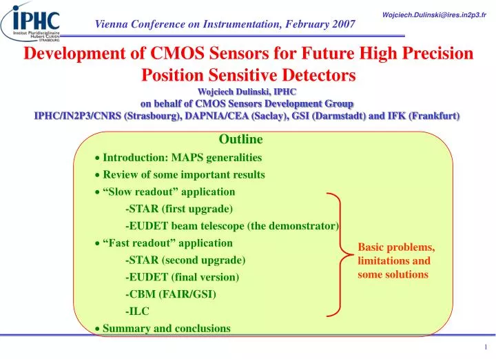
Development of CMOS Sensors for Future High Precision Position Sensitive Detectors. Wojciech Dulinski, IPHC on behalf of CMOS Sensors Development Group IPHC/IN2P3/CNRS (Strasbourg), DAPNIA/CEA (Saclay), GSI (Darmstadt) and IFK (Frankfurt). Outline Introduction: MAPS generalities

E N D
Development of CMOS Sensors for Future High Precision Position Sensitive Detectors Wojciech Dulinski, IPHCon behalf of CMOS Sensors Development Group IPHC/IN2P3/CNRS (Strasbourg), DAPNIA/CEA (Saclay), GSI (Darmstadt) and IFK (Frankfurt) • Outline • Introduction: MAPS generalities • Review of some important results • “Slow readout” application -STAR (first upgrade) -EUDET beam telescope (the demonstrator) • “Fast readout” application -STAR (second upgrade) -EUDET (final version) -CBM (FAIR/GSI) -ILC • Summary and conclusions Basic problems, limitations and some solutions
vdd vdd reset vdd select vdd select output output Standard 3T pixel cell gnd Self-biased pixel cell gnd CMOS Active Pixel Sensors for radiation (light) imaging, as a competitor to CCD: late 80’s E. R. Fossum, “CMOS image sensors: electronic camera-on-a-chip”, IEEE Trans. On Electron Devices 44 (10) (1997) Basic pixel electronics schemes (photodiode, 3 or 4 transistors, transfer gate…) : all this elements are still bases of today’s digital cameras Strasbourg (IReS/LEPSI) invention, well suited for particle tracking application
From digital cameras to particle tracking: use of an epitaxy layer as a detector active medium B. Dierickx, G. Meynants, D. Scheffer “Near 100% fill factor CMOS active pixel sensor”, Proc. of the IEEE CCD&AIS Workshop, Brugge, 1997 Twin - tub (double well), CMOS process with epitaxial layer • Charge generated by the impinging particle is collected by the n-well/p-epi diode. • Active volume is underneath the readout electronics allowing a 100% fill factor. • The active volume is NOT fully depleted: the effective charge collection is achieved through the thermal diffusion mechanism. • Doping gradient (P++substrate – P-epi – P+well) results in a potential minimum in the middle of epitaxy layer, limiting charge spread (2D instead of 3D) • The device can be fabricated using almost any standard, cost-effective and easily available CMOS process
Signal processing: Correlated Double Sampling in case of serial (slow) and column-parallel (fast) readout CDS: Signal = Sample(t1) – Sample (t0); t1-t0 is the integration time Serial (pixel-by-pixel) readout Column parallel (line-by-line) readout Line select Line select Analog Output Discrimination (or A-D conversion) Row select Zero suppression Digital CDS: after data digitization Analog CDS: before data digitization Sparsified, digital data output CDS is very efficient (and the only effective?) way of removing the inter-pixel pedestal spread, which is at least order of magnitude higher than the signal
Mimosa9 (various pitch) beam tests results (THE reference) AMS 0.35 µm CMOS OPTO process • Advanced mixed-signal polycide gate CMOS: 4 metal, 2 poly, high-res poly, 3.3V and 5V gates- Optimized N-well diode leakage current- 14 µm epi substrate (20 µm possible)- Availability through multi-project submissions, with a reasonable pricing (< 1 k€/mm2). In production, the price is of few k€ per 8 inch wafer. Signal in the seed pixel: down to few tens of electronsBut: ENC ~10 electrons,so S/N comfortableEfficiency >99.5%, for the fake hit rate ~10-5Excellent spatial resolution!
Applications of MAPS in particle physics experiments:slow (serial, analog) readout • STAR VxD upgrade 2008: 9+24 ladders • (analog) readout time = integration time = 2 - 4 ms • Room temperature operation (chip at ~ ≤40°C) • Air cooling only • Ionizing radiation dose:~8 krad/year (3 1011 p/cm2/year) • The Ultimate Upgrade: luminosity up, dose accordingly higher , integration time ~10x shorter. • Considered solution is based serial readout for the first upgrade and on column-parallel binary readout for the Ultimate Upgrade R = 2.5 and 7 cm L = 20 cm
Radiation tolerance for integrated ionizing dose: dark current increase Shot Noise Contribution @ 30°C and @4 ms integration time ENCshot = 39 electrons ENCshot = 12 electrons Standard N-well/p-epi diode dark current increase after irradiation with a 60Co g source (Mimosa9)
“Thin-oxide” diode dark current increase after irradiation with a 60Co g source standard diode layout Recent results (Mimosa15): x10 current increase after 1Mrad.Compatible with ILC requirements. thin-oxide diode layout
MimoSTAR-2 (30 µm pitch): the demonstrator for STAR experiment microvertex upgrade. Based on radiation tolerant N-well collecting diodes. JTAG based control and bias setting. S/N vs. dose
Mimo*2 beam tests: efficiency after irradiation Efficiency vs. dose, for S/N cuts = 5 (seed) and 2 (crown) After 47 kRads, efficiency >99 % at room temperature AND long (4ms) integration time, for the fake hits rate <10-4
Applications of MAPS in particle physics experiments:slow (serial, analog) readout • EUDET General Purpose Beam Telescope • Compact: to be mounted inside existing magnets, transportable • User friendly, easy to run AND to interface with various users • Sensitive area: few. sq. cm (at least 2 cm in one direction) • High precision tracking: down to ~1 µm in the center, also at medium energy beams (~ few GeV) Optional high-precision plane: 1 µm resolution Telescope resolution study: Analytical Track FittingMethod with Multiple Scattering, verified using GEANT 4 (credit to A.F.Zarnecki, Warsaw University)
Sensor fabrications in 2006: engineering run in AMS-0.35 OPTO • Motivated by MIMOSTAR-3 : 200 kpixels, tr.o. = 2 ms, 2 cm2 • Other chips: • MimoTEL: 0.8x0.8 cm2, rad.tol., 800 μs (EUDET) • IMAGER-10µ (M-18): expected resolution <1 μm (EUDET) • MIMOSA-16: binary readout architecture (EUDET, CBM, ILC) • Imager-12µ (M-19): charge-spread reduction • Low resolution, low power ADCs • Epitaxy thickness: 14 and 20 µm Almost all sensors have been tested and are working with promising performances, waiting for the beam tests in 2007…
Applications of MAPS in particle physics experiments:fast, column parallel, digital readout • CBM vertex detector (FAIR/GSI) • Readout time = integration = time resolution: <10 µs • Binary readout, no zero suppression • Vacuum operation • Ionizing radiation dose: >2 MRad • Neutron fluence (1MeV eq.):>1013 n/cm2 • Total single layer thickness: <150 µm (Si) Extremely demanding application, but no alterative solution candidates…
Mimosa8 (TSMC-0.25µ, 8 µm epi) – a binary readout demonstrator • CDS in pixel, based on “clamping” circuit solution • On-chip FPN suppression • Offset compensated comparator at the end of each column • Pixel pitch 25 x 25 µm2 Prototype in collaboration with Dapnia/Saclay
Mimosa8 beam tests results Comparator voltage scan (all pixels) • Output noise: 0.9 mV (ENC = 15 electrons) • Pixel-to-pixel FPN: 0.45 mV (7.5 electrons) • Spatial resolution: sr = ~7 µm • First demonstration of feasibility of FPN correction using on-chip real time circuitry • The design goal confirmed by the beam tests results: efficiency > 99 % • Second version (Mimosa16) in AMS-035 OPTO with 14 and 20 µm epi under test
Pixel optimization: diode size ↑ , charge collection ↑but also parasitic capacity and ENC ↑ ! Examples from measurements using recent AMS-035 OPTO test structures. Improved load Self-biasing CS, 2.4x2.4 µm diode ENC = 12 e, G = 65 µV/e Charge coll. eff. <25% CSFb, 4.5x4.5 µm diode ENC = 15 e, G =45 µV/e Charge coll. eff. >50% CAFb, 4.5x4.5 µm diode ENC = 12 e, G =65 µV/e Charge coll. eff. >50% * Collection efficiency: charge collected in 3x3 cluster, measured on 20 µm thick epi wafer and 25 µm pixel pitch
Radiation tolerance for the bulk damage: neutron irradiation Mimosa15 (AMS-035 OPTO), rad-tol diodes Mimosa15 MIP detection efficiency Charge loss observed after ~1012 n/cm2, correlated to the diode/pixel area ratio, seems to be rather basic and process independent. Going to smaller pitch and larger diodes (L-shaped) may bring some improvements (factor of two or three).
Possible (substantial) improvement B. Dierickx “Multiple or graded epitaxial wafers for particle or radiation detection”, US Patent 6,683,360 B1, Jan. 2004 PLUS deep implants available in some BiCMOS processes Field shaping using doping gradient faster charge collection smaller sensitivity to the bulk damage Field shaping smaller charge spread optimum conditions for the binary readout small shallow Nwell • Example from our simulationof novel MAPS structure (ISE TCAD, realistic doping profiles). In parentheses, typical standard structure. • Charge collection time: < 10 ns (~100ns) • Charge spread suppression: • > 60% (<30%) of charge in central pixel, all charge inside < 4 pixels (>9 pixels) • Prototypes in construction! shallow Pwell deep P_Inplant graded epitaxy substrate 12 µm
Thick metal for interconnection (busing) SOI CMOS or BiCMOS, digital processing @ data transmission, 10 µm thick Graded epitaxial wafer, MAPS layer, 20 µm thick CVD diamond, heat dissipation to periphery,50 to 100 µm thick Exploring new possibilities for MAPS performance upgrade, based on Vertical Integration (3D Electronics) industrial process. Vertical Integration ingredients: -Wafers thinning down to 10-20 µm ( flexible sheet!) - Precision alignment and molecular bonding of several layers -Through-wafer vias formation for electrical interconnection Result: 3D, monolithic circuit (or a sensor system) Possible applications in tracking systems: • Construction of monolithic ladder, integrating two active silicon layers (one full plane, stitched MAPS, plus one signal processing and transmission layer) bonded to heat dissipation, diamond layer. Total thickness < 150µm proposal for CBM application • Increased flexibility for wafer choice: post-processing step. Back-thinning and back-contact re-implementation at low temperature is possible, allowing an optimized use of thick, high-resistivity wafers available in many RF deep-submicron CMOS processes
Applications of MAPS in particle physics experiments:fast, column parallel, digital readout with low resolution ADCs • ILC VxD • Beam train: ~1 ms every ~200 ms • Outer layers integration time: < ~200 µs • Inner layers integration time: < ~25 - 50 µs • Neutron eq. fluence: < ~1010 neq/cm2/year • Ionizing dose: <50 krad/year (~10 MeV electrons) Real data based simulation of MAPS tracking performance versus end-of-column ADC resolution, supposing efficient (analog) FPN suppression
Conclusions • Monolithic CMOS Pixels Sensors, after several years of development, starts to reach certain maturity level. However, there is still a room for substantial improvements within existing technologies. In particular, deep-submicron, triple-well CMOS (or BiCMOS) processes should be better explored and evaluated. The use of commercial, easily available and cheap technology is a great thing not only for prototyping but also for large scale production!For applications requiring ultra-thin sensors and ultra-high spatial resolution in relatively large area, MAPS are the leading candidates. First applications in physics experiments are expected soon and will be (probably) crucial for this technique. Each application requires careful optimization, but this is possible – MAPS are ASICS! Commercial technology advances, like apparition and availability of Vertical Integration, may also allow for important upgrade of MAPS performances and increase flexibility of system aspects.
Back-up slides: Calibration of the conversion gain - with soft X-rays • Calibration methods: • Emission spectra of a low energy X-ray source e.g. iron 55Fe emitting 5.9 keV photons. • very high detection efficiency even for thin detection volumes - =140 cm2/g, constant number of charge carriers about 1640 e/h pairs per one 5.9 keV photon MIMOSA I (14 m EPI) configuration with single diode in one pixel MIMOSA I (14 m EPI) configuration with four diodes in one pixel The ‘ warmest ’ colour represents the lowest potential in the device
Back-up slides:The simplest readout electronics: diode + 3 transistors/pixel • Reset in order to inverse bias • Continuous serial addressing and readout (digitisation) of all pixels • Keeping two successive frames in external circular buffer • Following reset when needed (removing integrated dark current) • After trigger (or in a real time)), simple data processing in order to recognise hits Fast ADC 12 bits Buffer : 512 words/channel %trigger ! F0 F1 256 kwords 256 kwords
Back-up slides:Data processing: (Digital) Correlated Double Sampling ( ) - Useful signal on top ofFixed Pattern DC level Fixed Pattern dispersion: ~100 mV Typical signal amplitude: ~1mV (frame2 - frame1) subtraction ( ) - Pedestal (dark current) subtraction Hit candidates!
Back-up slides:A “typical” example from the beam tests: 30µm pitch array, 20°C Signal in the seed pixel: down to few tens of electrons ENC: ~10 electrons Efficiency >99%, spatial resolution: down to 1.5 µm
Back-up slides:Fe55 spectrum before (red) and after (green) 1 Mrad of X-rays @40°C (200 µs integration) : prove of principle for ILC Rad-tol central pixel Rad-tol 4-pixel cluster Standard 4-pixel cluster