Download

1 / 31
310 likes | 379 Views
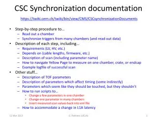
CSC Synchronization Procedure and Plans. CMS Endcap Muon meeting @ FNAL October 29, 2004 Jay Hauser* / Martin Von der Mey / Yangheng Zheng University of California, Los Angeles. What is done now What should be done. General ~Trigger-Centric View.

E N D
CSC Synchronization Procedure and Plans CMS Endcap Muon meeting @ FNAL October 29, 2004 Jay Hauser* / Martin Von der Mey / Yangheng Zheng University of California, Los Angeles What is done now What should be done
General ~Trigger-Centric View • Adjust transmit/receive phases within 25ns base period to get proper data transmission between boards • Adjust L1A time to get fixed 2.9us for CFEB-L1A (not possible in CMS, hard for slice test) • Put trigger and readout signals in the middle of numerous several-bx time coincidence windows on ALCT, TMB, DMB • Adjust ALCT fine delay timing to get events in ~1 bx (for synchronous or semi-synchronous beam) • Equalize time of arrival of signals at SP • Equalize BX numbers for DAQ readout Endcap Muon meeting @ FNAL
Step 1: Adjusting Clock Phases • TMB has several adjustments: • CFEB-TMB has “receive” phase • ALCT-TMB has “transmit” and “receive” phases • Use CFEB pulse injection • Use test strip pulses to pulse wires Endcap Muon meeting @ FNAL
TMB-CFEB Block Diagram TMB Crate Master clock TMB Master clock Latch data in CLCT section Comp. delay Data Delay Devices 2ns/bin 40 MHz clock Comparator data CFEB (1 of 5) • Clock and data on same 6-15m Skewclear cable • Adjust comparator clock phase to middle of ~12ns window where data is latched correctly by TMB Comparators
Active Pulsing of CFEB Front Ends • Generate ½ -strip patterns for all layers: • Buckeye ASIC - all channels have capacitors with 4 charge levels that can be preset (0,1,2,3) • “left half-strip” puts strip charges at ….,0,0,2,3,1,0,0… • “right half-strip” puts strip charges at …,0,0,1,3,2,0,0… • Single VME command to DMB pulses all channels simultaneously • Patterns give e.g. 6-layer CLCTs • First vary 40 MHz clock phase from TMB to comparators until patterns correctly found • Then patterns can be swept across entire chamber and checked • Checks all Buckeye, comparator, and CFEB-TMB Skewclear cable channels • No gas, HV, etc. needed Endcap Muon meeting @ FNAL
CFEB Clock Phase Determination Endcap Muon meeting @ FNAL
CFEB Pulse Pattern Injector Endcap Muon meeting @ FNAL
Active Pulsing of Test Strips • How it’s done: • CCB provides 500ns gate to make the ALCT test strip pulses • Capacitive coupling between test strips and anode wire groups gives pulses on leading and trailing edges of 500ns pulse • All channels fire on leading edge • Hot wire mask on ALCT board ALCT patterns • Like CFEB, vary 40 MHz receive and send phases until optimum data transmission from TMB to and from ALCT • Find optimum in 2D matrix of receive/send clock phases • Scan patterns across chamber to find bad AFEB/ALCT channels • Advantages: • Set up phases of 80 MHz clock TMB to and from ALCT with high reliability without HV, gas, or cosmic ray data • Check all AFEB, ALCT, and Skewclear channels through the system • What previously took days now takes minutes Endcap Muon meeting @ FNAL
TMB-ALCT Block Diagram TMB ALCT section ALCT AFEB Crate Master clock TMB Master clock Latch input ALCT data • Adjust ALCTtx for optimal latching of ALCT output data at TMB 2ns/bin Latch output ALCT commands ALCT -RX clock CCB test pulse commands • Adjust ALCTrx for optimal latching TMB output data at ALCT ALCT -TX clock TMB pass- through 2ns/bin ALCT commands ALCT data ALCT Master clock ALCT Main FPGA • Adjust Delay ASICs for max. probability for ALCTs to come in one BX Internal test pulse via VME command to TMB Asynch. test pulse from VME write to CCB Delay ASICs ALCT latch raw data Synch. test pulse from TTC command or VME write to CCB Main FPGA OR ~2.2ns/bin CSC Test Pulse Strips AFEB data Test pulse to AFEB amplifier or test strips (select via VME write to TMB to ALCT Slow Control FPGA register)
ALCT Clock Phases Determination Good settings Endcap Muon meeting @ FNAL
AFEB Pulse Pattern Injector Endcap Muon meeting @ FNAL
Step 2: Adjusting L1A at CFEBs • Firmware in CFEBs uses L1A delay at 2.9us • So far, experts adjust DMB timing according to observations with oscilloscope at CFEB • Difficult but possible for slice tests • Impossible in situ for CMS • CMS plan: calculate cable lengths etc. and have firmware for all required delays • Is this good enough? Endcap Muon meeting @ FNAL
Step 3: Putting Signals in Windows Most important settings: • On DMB: TMB pretrigger to L1A delay • For CFEB readout. Use DMB front-panel gizmo to set. • On ALCT: L1A delay • Initiates readout. Use TMB scope. • On CLCT: L1A delay • Initiates readout. Use TMB scope. • On TMB: ALCT-CLCT coincidence delay • For matched LCT to MPC. Can use TMB scope or DQM, etc. • On TMB: RPC-LCT coincidence delay • For matched RPC to LCT (if desired). Use TMB scope or DQM. • On DMB: ALCT data-available to L1A delay • For ALCT FIFO readout. Scan until ALCTs read out efficiently. • On DMB: CLCT data-available to L1A delay • For CLCT/TMB FIFO readout. Scan until CLCTs read out efficiently. Etc. etc. Endcap Muon meeting @ FNAL
TMB-DMB Block Diagram TMB DMB CFEB TTC/CCB Crate Master Clock, L1A • (external L1A = LHC & Test Beam operation modes) TMB Master Clock, L1A DMB Master Clock, L1A CLCT DAV delay L1A*CLCT DAV Coinc. CLCT-DAV LCT-L1A Coinc. starts TMB readout CLCT Readout queue CLCT FIFO DMB-DDU readout Controller logic ALCT DAV delay L1A*ALCT DAV Coinc. ALCT-DAV LCT -read delay LCTs to MPC From ALCT readout queue ALCT FIFO CFEB DAV Coinc. CFEB Clock phase L1A delay L1A ALCT/ CLCT/ RPC Coincidence RPC delay 1 ns/bin CFEB DAV delay CFEBs “hit” Auto set Cable Equal. delay AFF (Active FEB Flags) Cable Equal. delay CFEB FIFOs (5) CFEB -DAV CLCT Final logic AFF-L1A Coinc. Starts CFEB digi. & readout RPC logic AFF delay ALCT delay Output FPGA fixed CFEB Clock SCAs, ADCs, Memories From RPC/ RAT Store SCA data command From ALCT CLCT pre-trigger logic Comparators
Step 4: Adjust ALCT Fine Timing Clock Gate Accepted Scint. Coinc. • Scan 0-25 ns delays in 2.2ns steps • Try to get >99% or so of ALCTs in 1 bx • Works well for synchronous beam • Doesn’t work well for cosmics/asynchronous beam • Big improvement to set up synchronous gating during asynchronous test beam: • Sometimes delay setting moves ALCTs to a different bx window back to previous step for iteration. • N.B. In CMS will need several adjustments per chamber (TOF varies by ~6ns, also cable delays) Endcap Muon meeting @ FNAL
Step 5. Equalize time of arrival of LCTs at SP • All chambers in crate must be equalized • (to the slowest) • Then the various crates must be equalized • (to the slowest!) • Then need to equalize with Drift Tube LCTs • For overlap-region muons • (whichever is slowest!) • Simple adjustment in TMB to delay signals • At test beam, used long input FIFO of SP (?) Endcap Muon meeting @ FNAL
Step 6. Equalize BX numbers for DAQ readout • Also low-order bits go to SP • Never properly worked out at test beam • Different boards used different algorithms: • DMB, CFEB, DDU reset on BC0 • ALCT, CLCT reset on BXReset only • Orbit was not reliably 924 crossings • RPCs used LHC orbit (3564 or something) Endcap Muon meeting @ FNAL
Eventual LHC Operation • Many synchronizations are done easily with real LHC beams • Synchronous beam • Rate is high • Cabling is “permanent” • There are easy-to-find gaps in the orbit structure • Can turn on with one bunch per orbit, for example (Wesley) Endcap Muon meeting @ FNAL
Eventual LHC Operation • However: • We will want to exercise a working system long before LHC turn-on • There are 486 chambers to time in • The trigger has to be timed to the very slowest chamber (longest TOF+cable runs, etc.) • Chambers and even peripheral crates are inaccessible • There could be long-term shifts in timing – constant automated monitoring is advisable • How to do large-scale slice test at SX5? • How to do anything after disks lowered but still <<LHC?? Endcap Muon meeting @ FNAL
Summary • Synchronization is pretty hard • I’ve certainly overlooked a lot of steps • Any improvements in synchronization “technology” will pay off big-time • (Lev’s BC0 handling for trigger path?) • It would be nice to automate more of the currently manual procedures • Timing diagrams updated at http://www.physics.ucla.edu/~hauser/CSC_peripheral_timing.ppt Endcap Muon meeting @ FNAL
Additional Slides Follow Endcap Muon meeting @ FNAL
CSC Peripheral Crate Timing04-Mar-2004 • This note at http://www.physics.ucla.edu/~hauser/CSC_peripheral_timing.ppt • TTC distribution to peripheral crate cards • TMB-CFEB diagram • TMB-ALCT diagram • Details of L1A-LCT coincidences in TMB & DMB • TMB clocking to MPC • (CCB-TTC clocking details)
Master Clock Distribution inCSC Peripheral Crates CCB TTC Phase adjustment 0.1 ns/bin (unused so far) TTCrx Crate Master clock: Isochronous backplane distribution … TMB 1 DMB 1 TMB 9 DMB 9 MPC • TTC command and data strobes are delayed along with the phase adjustment so as to remain within 25ns latch window
TMB-CFEB Block Diagram TMB Crate Master clock TMB Master clock Latch data in CLCT section Comp. delay Data Delay Devices 2ns/bin 40 MHz clock Comparator data CFEB (1 of 5) • Clock and data on same 6-15m Skewclear cable • Adjust comparator clock phase to middle of ~12ns window where data is latched correctly by TMB Comparators
TMB-ALCT Block Diagram TMB ALCT section ALCT AFEB Crate Master clock TMB Master clock Latch input ALCT data • Adjust ALCTtx for optimal latching of ALCT output data at TMB 2ns/bin Latch output ALCT commands ALCT -RX clock CCB test pulse commands • Adjust ALCTrx for optimal latching TMB output data at ALCT ALCT -TX clock TMB pass- through 2ns/bin ALCT commands ALCT data ALCT Master clock ALCT Main FPGA • Adjust Delay ASICs for max. probability for ALCTs to come in one BX Internal test pulse via VME command to TMB Asynch. test pulse from VME write to CCB Delay ASICs ALCT latch raw data Synch. test pulse from TTC command or VME write to CCB Main FPGA OR ~2.2ns/bin CSC Test Pulse Strips AFEB data Test pulse to AFEB amplifier or test strips (select via VME write to TMB to ALCT Slow Control FPGA register)
TMB-ALCT Timing Discussion I • Definitions: • T=Skewclear cable and buffer delay (~30-75ns) • dtRX=adjustable delay time for ALCTrx • dtTX=adjustable delay time for ALCTtx • Let phase of TMB master clock be defined as =0 • Then Step 1 of timing-in optimizes data transfer from ALCT to TMB: • ALCT data to TMB is received (latched) in the TMB at phase=0. • ALCT data to TMB is sent (latched) at the ALCT at phase=mod[T+ dtTX, 25ns]. • Step 2 of the timing-in procedure optimizes commands from TMB to ALCT: • TMB commands to ALCT are sent (latched) in the TMB at phase= mod[dtRX, 25ns]. • TMB commands to ALCT are received (latched) at the ALCT at phase=mod[T+ dtTX, 25ns]. • Since the latter depends on dtTX, this procedure must be done after Step 1.
TMB-ALCT Timing Discussion II Possible hole e Nominal window dtRX • Note bene: there are certain values of dtRX that can cause meta-stable TMB output latching (those that are close to 25ns boundary between TMB internal clock cycles). • Therefore, it may be necessary to iterate Steps 1 and 2 to find the widest time windows for simultaneous data transfer in both directions. • Note that DDD (new) and PHOS4 (old) delay chips both have t0’s that vary chip-to-chip, so the phase of the hole varies between TMBs. • Once this is set, it is then necessary to adjust integer-BX delays and timing windows on ALCT, TMB, and DMB for L1A coincidence to ensure efficient triggering and readout.
TMB-ALCT Timing Discussion III • Final step of phase adjustment procedure after TMB-ALCT communication is optimized: • Adjust ALCT Delay ASICs to get the maximum probability for ALCTs to come in one BX. • In case of LHC or structured beam, this is easy based on data analysis. • In case of asynchronous cosmic rays or test beam: • This is meaningless except for trying to get good relative timing between multiple chambers. • One can use scintillators and a coincidence with a short pulse (few ns) synchronized with the peripheral crate clock to get semi-synchronous external cosmic ray trigger.
TMB-DMB Block Diagram TMB DMB CFEB TTC/CCB Crate Master Clock, L1A • (external L1A = LHC & Test Beam operation modes) TMB Master Clock, L1A DMB Master Clock, L1A CLCT DAV delay L1A*CLCT DAV Coinc. CLCT-DAV LCT-L1A Coinc. starts TMB readout CLCT Readout queue CLCT FIFO DMB-DDU readout Controller logic ALCT DAV delay L1A*ALCT DAV Coinc. ALCT-DAV LCT -read delay LCTs to MPC From ALCT readout queue ALCT FIFO CFEB DAV Coinc. CFEB Clock phase L1A delay L1A ALCT/ CLCT/ RPC Coincidence RPC delay 1 ns/bin CFEB DAV delay CFEBs “hit” Auto set Cable Equal. delay AFF (Active FEB Flags) Cable Equal. delay CFEB FIFOs (5) CFEB -DAV CLCT Final logic AFF-L1A Coinc. Starts CFEB digi. & readout RPC logic AFF delay ALCT delay Output FPGA fixed CFEB Clock SCAs, ADCs, Memories From RPC/ RAT Store SCA data command From ALCT CLCT pre-trigger logic Comparators
TMB-DMB Timing Discussion I • 2.9 us for AFF to L1A now set manually by looking on oscilloscope at CFEB to adjust the L1A timing. At LHC L1A timing will be a fixed constant determined by the global CMS trigger. The firmware on the CFEB contains a fixed pipeline (not adjustable). • TMB knobs (default settings): • ALCT-CLCT coincidence delay for ALCT (8 bx), width (3 bx) • RPC-CLCT coincidence delay for RPC (20 bx?), width (1 bx?) – to be determined. • L1A coincidence delay (128=0x80 bx), width (3 bx) • DMB knobs (default settings): • AFF-to-L1A delay (116 bx), coincidence width (3 bx) • L1A to CFEB-DAV (Data Available) delay (0x18 bx), coincidence width (2 bx) • L1A to ALCT-DAV (Data Available) delay (4 bx), coincidence width (2 bx) • L1A to CLCT-DAV (Data Available) delay (0x15 bx), coincidence width (2 bx) • CFEB Cable Equalization delay (0 bx) – to be added
TMB-MPC Block Diagram TMB MPC … Crate Master 40 & 80 MHz clocks TMB Master clock MPC Master 40 &80 MHz clocks DLL makes 80 MHz, phase=0 80 MHz VCX0 Winner Bits 40 MHz Optical to Track Finder at 80 MHz Select Winner bits pointer MPC Master phase ALCT-CLCT-RPC coincidence logic LCT Readout Controller 0.25 ns/bin Sort best 3/18 logic LCTs at 80 MHz on backplane Clk. Mult. to 80 MHz 40-to-80 MHz MUX Latch and de-mux TMB LCT data • MPC Latch Delay is adjusted to middle of latch window for data from all 9 TMBs. • Winner bits come back to TMB about 8 clock cycles after LCTs sent to MPC (Pointer to data in pipeline should be fixed for all time) • Phase of Winner bits to TMB may need adjustment on TMB end.