Download
1 / 22
250 likes | 701 Views
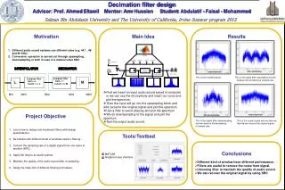
5-bit Decimation Filter. Loretta Chui, Xiao Zhuang Hock Cheah, Gita Kazemi Advisor: David Parent December 6, 2004. Agenda. Abstract Introduction Project Details Results Cost Analysis Conclusions. Abstract.

E N D
5-bit Decimation Filter Loretta Chui, Xiao Zhuang Hock Cheah, Gita Kazemi Advisor: David Parent December 6, 2004
Agenda • Abstract • Introduction • Project Details • Results • Cost Analysis • Conclusions
Abstract • We designed a 5-bit Decimation Filter, which can be used to sample the output of an A/D converter at a lower rate. Our system operates at 143 MHz, uses less than 100 mW of power, and occupies an area of 360 x 280 mm2.
Introduction • The averaging filter used at the output of an A/D converter is called a decimation filter. • The decimation filter samples the incoming data until the sum of k inputs has been accumulated. Then, the sum is dumped into an output flip-flop. Through this process, the filter reduces (decimates) the output frequency by k times.
Impulse Output Impulse Input Step Output Step Input
DFF Fall Time For Hold DFF Rise Time For Hold
DFF Fall Time for Setup DFF Rise Time for Setup
Cost Analysis • Estimated time spent on each phase of the project: • verifying logic (1 week) • verifying timing (1 week) • layout (3 weeks) • post extracted timing (1.5 weeks)
Conclusion • We designed a decimation filter, which samples and sums the incoming data 3 inputs at a time. Through this process, the filter reduces (decimates) the output frequency by a factor of 3. • Our design met all specifications except for timing because our adder was too slow. • We propose the use of an alternative design, which uses a mux select to implement a faster adder.
Lessons Learned • It would be helpful to students to use a layered approach for the chip layout by creating instances of individual parts instead of copy and paste to improve debugging capabilities. • It would be helpful if professors could spend some time to cover testing methodology.
Acknowledgements • Thanks to our family and friends who missed us for the past 3 months. • Thanks to Cadence Design Systems for the VLSI lab. • Thanks to Dr. Parent and John for their advice and great patience.