Download
1 / 51
510 likes | 537 Views
Learn about write-back vs. write-through cache, allocation policies, cache coherence issues, and solutions in modern Intel processors. Understand memory system behavior and cache hierarchy for efficient programming.

E N D
Lecture 10: Snooping-Based Cache Coherence
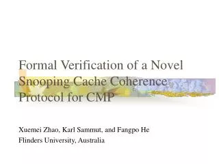
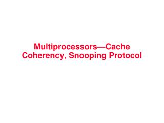
Line state Tag Cache design review Data (64 bytes on modern Intel processors) Dirty bit Let’s say your code executes volatile int x = 1; • Review: • What is the difference between a write back and a write-through cache? • What about a allocate vs. write-no-allocate cache? (Assume for simplicity x corresponds to the address 0x12345604 in memory—it’s not stored in a register) One cache line: . . . 1 0 0 0 Byte 0 of line Byte 63 of line
Line state Data (64 bytes on modern Intel processors) Tag Review: behavior of write-allocate, write-back cache on a write miss (uniprocessor case) Dirty bit Example: processor executes volatile int x = 1; Processor performs write to address that is not resident in cache Cache selects location to place line in cache, if there is a dirty line currently in this location, the dirty line is written out to memory Cache loads line from memory (“allocates line in cache”) 4 bytes of cache line are updated Cache line is marked as dirty
A shared memory multi-processor Processor Processor Processor Processor Memory I/O • Processors read and write to shared variables • More precisely: processors issue load and store instructions • A reasonable expectation of memory is: • Reading a value at address X should return the last value written to address X by any processor Interconnect (A simple view of four processors and their shared address space)
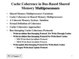
0 1 P3 load X P3 store X P2 load X 2 0 2 1 0 P1 store X 1 0 miss hit 1 1 0 0 0 2 miss 0 0 0 P1 load X 0 0 Cache Cache Cache Cache Processor Processor Processor Processor Memory The cache coherence problem P2 load X 0 0 miss 0 Modern processors replicate contents of memory in local caches Problem: processors can observe different values for the same memory location Interconnect int foo; (stored at address X) Action P1 $ P2 $ P3 $ P4 $ mem[X] The chart at right shows the value of variable foo (stored at address X) in main memory and in each processor’s cache Assume the initial value stored at address X is 0 Assume write-back cache behavior 0 P1 load Y (assume this load causes eviction of X)
Cache Cache Cache Cache Processor Processor Processor Processor Memory The cache coherence problem Interconnect Is this a mutual exclusion problem? Can you fix the problem by adding locks to your program? NO! This is a problem created by replicating the data stored at address X in local caches (a hardware implementation detail) int foo; (stored at address X) Action P1 $ P2 $ P3 $ P4 $ mem[X] The chart at right shows the value of variable foo (stored at address X) in main memory and in each processor’s cache Assume the initial value stored at address X is 0 Assume write-back cache behavior 0 miss P1 load X 0 0 P2 load X 0 0 miss 0 P1 store X 1 0 0 miss P3 load X 1 0 0 0 P3 store X 1 0 2 0 hit P2 load X 1 0 2 0 P1 load Y (assume this load causes eviction of X) 0 2 1
The memory coherence problem • Intuitive behavior for memory system: reading value at address X should return the last value written to address X by any processor. • Memory coherence problem exists because there is both global storage (main memory) and per-processor local storage (processor caches) implementing the abstraction of a single shared address space.
Shared L3 Cache (One bank per core) Cache hierarchy of Intel Haswell CPU (2013) 64 byte cache line size L3: (per chip) 8 MB, inclusive 16-way set associative 32B / clock per bank 26-31 cycle latency Ring Interconnect L2: (private per core) 256 KB 8-way set associative, write back 32B / clock, 12 cycle latency Up to 16 outstanding misses L2 Cache L2 Cache L2 Cache L2 Cache L1: (private per core) 32 KB 8-way set associative, write back 2 x 16B loads + 1 x 16B store per clock 4-6 cycle latency Up to 10 outstanding misses L1 Data Cache L1 Data Cache L1 Data Cache L1 Data Cache Core Core Core Core
Intuitive expectation of shared memory • Intuitive behavior for memory system: reading value at address X should return the last value written to address X by any processor. • On a uniprocessor, providing this behavior is fairly simple, since writes typically come from one client: the processor • Load operation must examine all pending stores in store buffer • Exception: device I/O via direct memory access (DMA)
Cache Processor Network Card Memory Coherence is an issue in a single CPUsystem Consider I/O device performing DMA data transfer • Common solutions: • CPU writes to shared buffers using uncached stores (e.g., driver code) • OS support: • Mark virtual memory pages containing shared buffers as not-cachable • Explicitly flush pages from cache when I/O completes • In practice, DMA transfers are infrequent compared to CPU loads and stores (so these heavyweight software solutions are acceptable) Case 1: Processor writes to buffer in main memory Processor tells network card to async send buffer Problem: network card many transfer stale data if processor’s writes (reflected in cached copy of data) are not flushed to memory Case 2: Network card receives message Network card copies message in buffer in main memory using DMA transfer Card notifies CPU msg was received, buffer ready to read Problem: CPU may read stale data if addresses updated by network card happen to be in cache Interconnect Message Buffer
Problems with the intuition • Intuitive behavior: reading value at address X should return the last value written to address X by any processor. • What does “last” mean? • What if two processors write at the same time? • What if a write by P1 is followed by a read from P2 so close in time that it is impossible to communicate the occurrence of the write to P2 in time? • In a sequential program, “last” is determined by program order (not time) • Holds true within one thread of a parallel program • But we need to come up with a meaningful way to describe order across threads in a parallel program
Definition: coherence Chronology of operations on address X A memory system is coherent if: The results of a parallel program’s execution are such that for each memory location, there is a hypothetical serial order of all program operations (executed by all processors) to the location that is consistent with the results of execution, and: • Memory operations issued by any one processor occur in the order issued by the processor • The value returned by a read is the value written by the last write to the location… as given by the serial order P0 write: 5 P1 read (5) P2 read (5) P0 read (5) P1 write: 25 P0 read (25) Also known as sequential consistency
Definition: coherence (said differently) A memory system is coherent if: • A read by processor P to address X that follows a write by P to address X, should return the value of the write by P (assuming no other processor wrote to X in between) • A read by processor P1 to address X that follows a write by processor P2 to X returns the written value... if the read and write are “sufficiently separated” in time (assuming no other write to X occurs in between) • Writes to the same address are serialized: two writes to address X by any two processors are observed in the same order by all processors. (Example: if values 1 and then 2 are written to address X, no processor observes X having value 2 before value 1) Condition 1: obeys program order (as expected of a uniprocessor system) Condition 2: “write propagation”: Notification of a write must eventually get to the other processors. Note that precisely when information about the write is propagated is not specified in the definition of coherence. Condition 3: “write serialization”
Write serialization Writes to the same location are serialized: two writes to address X by any two processors are observed in the same order by all processors. (Example: if a processor observes X having value 1 and then 2, then no processor observes X having value 2 before it has value 1) Example: P1 writes value a to X. Then P2 writes value b to X. Consider situation where processors P3 and P4 observe different order of writes: Order observed by P3 ld X →load returns “a” ld X →load returns “b” Order observed by P4 ld X →load returns “b” ld X →load returns “a” ... ... • In terms of the first coherence definition: there is no global ordering of loads and stores to X that is in agreement with results of this parallel program. • (you cannot put the two memory operations involving X on a single timeline and have both processor’s observations agree with the timeline)
Implementing coherence • Software-based solutions • OS uses page-fault mechanism to propagate writes • Can be used to implement memory coherence over clusters of workstations • We won’t discuss these solutions • Hardware-based solutions • “Snooping”-based coherence implementations (today) • Directory-based coherence implementations (next week)
Processor Processor Processor Processor Cache Memory Shared caches: coherence made easy • One single cache shared by all processors • Eliminates problem of replicating state in multiple caches • Obvious scalability problems (since the point of a cache is to be local and fast) • Interference / contention due to many clients • But shared caches can have benefits: • Facilitates fine-grained sharing (overlapping working sets) • Loads/stores by one processor might pre-fetch lines for another processor I/O Interconnect
Cache Cache Cache Memory Processor Processor Processor Snooping cache-coherence schemes • Main idea: all coherence-related activity is broadcast to all processorsin the system (more specifically: to the processor’s cache controllers) • Cache controllers monitor (“they snoop”) memory operations, and react accordingly to maintain memory coherence Notice: now cache controller must respond to actions from “both ends”: LD/ST requests from its local processor Coherence-related activity broadcast over the chip’s interconnect . . . Interconnect
cache miss for X P1 load X P0 write 100 to X invalidation for X 100 100 100 100 100 Cache Cache . . . Processor P0 Processor P1 Memory Very simple coherence implementation • Let’s assume: • Write-through caches • Granularity of coherence is cache line • Upon write, cache controller broadcasts invalidation message • As a result, the next read from other processors will trigger cache miss • (processor retrieves updated value from memory due to write-through policy) Interconnect Action Interconnect activity P0 $ P1 $ mem location X 0 cache miss for X P0 load X 0 0 cache miss for X 0 0 0 P1 load X
A clarifying note • The logic we are about to describe is performed by each processor’s cache controller in response to: • Loads and stores by the local processor • Messages it receives from other caches • If all cache controllers operate according to this described protocol, then coherence will be maintained • The caches “cooperate” to ensure coherence is maintained • Cache controller tracks the status of each line in its cache
Write-through invalidation: state diagram • Two cache line states (same as meaning of invalid in uniprocessor cache) • Invalid (I) • Valid (V) • Two processor operations (triggered by local processor) • PrRd (read) • PrWr (write) • Two bus transactions (from remote caches) • BusRd (another processor intends to read line) • BusWr (another processor intends to write to line) PrRd / -- PrWr / BusWr V (Valid) PrRd / BusRd BusWr/-- I (Invalid) Notation: A / B: if event A is observed by cache controller, then action B is taken Remote processor (coherence) initiated transaction PrWr / BusWr ** Local processor initiated transaction ** Assumes write no-allocate policy (for simplicity)
Write-through invalidation: state diagram Requirements of the interconnect: All write transactions visible to all cache controllers All write transactions visible to all cache controllers in the same order Simplifying assumptions here: Interconnect and memory transactions are atomic Processor waits until previous memory operations is complete before issuing next memory operation Invalidation applied immediately as part of receiving invalidation broadcast PrRd / -- PrWr / BusWr V (Valid) PrRd / BusRd BusWr/-- I (Invalid) A / B: if action A is observed by cache controller, action B is taken PrWr / BusWr ** Remote processor (coherence) initiated transaction Local processor initiated transaction ** Assumes write no-allocate policy (for simplicity)
Write-through policy is inefficient • Every write operation goes out to memory • Very high bandwidth requirements • Write-back caches absorb most write traffic as cache hits • Significantly reduces bandwidth requirements • But how do we ensure write propagation/serialization? • This requires more sophisticated coherence protocols
Line state Data (64 bytes on modern Intel processors) Tag Recall cache line state bits Dirty bit
Cache Cache . . . Processor P0 Processor P1 Memory Cache coherence with write-back caches • Dirty state of cache line now indicates exclusive ownership • Exclusive: cache is only cache with a valid copy of line (it can safely be written to) • Owner: cache is responsible for supplying the line to other processors when they attempt to load it from memory (otherwise a load from another processor will get stale data from memory) Chronology of operations on address X Interconnect Load X Write to X P0 write P1 read X
Invalidation-based write-back protocol Key ideas: • A line in the “exclusive” state can be modified without notifying the other caches • Processor can only write to lines in the exclusive state • So they need a way to tell other caches that they want exclusive access to the line • They will do this by sending messages to all the other caches • When cache controller observes (via snooping) a request for exclusive access to line it contains • It must invalidate the line in its own cache • What if the line is dirty?
MSI write-back invalidation protocol • Key tasks of protocol • Ensuring processor obtains exclusive access for a write • Locating most recent copy of cache line’s data on cache miss • Three cache line states • Invalid (I): same as meaning of invalid in uniprocessor cache • Shared (S): line valid in one or more caches • Modified (M): line valid in exactly one cache (a.k.a. “dirty” or “exclusive” state) • Two processor operations (triggered by local CPU) • PrRd (read) • PrWr (write) • Three coherence-related bus transactions (from remote caches) • BusRd: obtain copy of line with no intent to modify • BusRdX: obtain copy of line with intent to modify • flush: write dirty line out to memory
MSI state transition diagram * A / B: if action A is observed by cache controller, action B is taken PrRd / -- PrWr / -- Remote processor (coherence) initiated transaction Local processor initiated transaction M (Modified) flush = flush dirty line to memory BusRd / flush PrWr / BusRdX S (Shared) BusRdX / flush PrWr / BusRdX PrRd / BusRd BusRdX / -- PrRd / -- BusRd / -- I (Invalid) * Remember, all caches are carrying out this logic independently to maintain coherence
Example Execution X and Y have value 0 at start of execution.
Summary: MSI • A line in the M state can be modified without notifying other caches • No other caches have the line resident, so other processors cannot read these values (without generating a memory read transaction) • Processor can only write to lines in the M state • If processor performs a write to a line that is not exclusive in cache, cache controller must first broadcast a read-exclusive transaction to move the line into that state • Read-exclusive tells other caches about impending write (“you can’t read any more, because I’m going to write”) • Read-exclusive transaction is required even if line is valid (but not exclusive… it’s in the S state) in processor’s local cache (why?) • Dirty state implies exclusive • When cache controller snoops a “read exclusive” for a line it contains • Must invalidate the line in its cache • Because if it didn’t, then multiple caches will have the line (and so it wouldn’t be exclusive in the other cache!) • And supply line value to requesting cache controller
Does MSI satisfy coherence? • Write propagation • Achieved via combination of invalidation on BusRdX, and flush from M-state on subsequent BusRd/BusRdX from another processors • Write serialization • Writes that appear on interconnect are ordered by the order they appear on interconnect (BusRdX) • Reads that appear on interconnect are ordered by order they appear on interconnect (BusRd) • Writes that don’t appear on the interconnect (PrWr to line already in M state): • Sequence of writes to line comes between two interconnect transactions for the line • All writes in sequence performed by same processor, P (that processor certainly observes them in correct sequential order) • All other processors observe notification of these writes only after a interconnect transaction for the line. So all the writes come before the transaction. • So all processors see writes in the same order.
MESI invalidation protocol • MSI requires two interconnect transactions for the common case of reading an address, then writing to it (why is this common?) • Transaction 1: BusRd to move from I to S state • Transaction 2: BusRdX to move from S to M state • This inefficiency exists even if application has no sharing at all • Solution: add additional state E (“exclusive clean”) • Line has not been modified, but only this cache has a copy of the line • Decouples exclusivity from line ownership (line not dirty, so copy in memory is valid copy of data) • Upgrade from E to M does not require an interconnect transaction
MESI state transition diagram PrRd / -- PrWr / -- M (Modified) PrWr / -- E (Exclusive) BusRd / flush PrWr / BusRdX BusRd / -- BusRdX / flush PrWr / BusRdX PrRd / -- S (Shared) PrRd / BusRd (no other cache asserts shared) PrRd / BusRd BusRdX / -- BusRdX / -- PrRd / -- (another cache asserts shared) BusRd / -- I (Invalid)
Example Execution X and Y have value 0 at start of execution.
Lower-level choices • Who should supply data on a cache miss when line is in the E or S state of another cache? • Can get cache line data from memory or can get data from another cache • If source is another cache, which one should provide it? • Cache-to-cache transfers add complexity, but commonly used to reduce both latency of data access and reduce memory bandwidth required by application
Increasing efficiency (and complexity) • MESIF (5-state invalidation-based protocol) • Like MESI, but one cache holds shared line in F state rather than S (F=”forward”) • Cache with line in F state services miss • Simplifies decision of which cache should provide block on miss (basic MESI: all caches respond) • Used by Intel processors • MOESI (5-state invalidation-based protocol) • In MESI protocol, transition from M to S requires flush to memory • Instead transition from M to O (O=”owned, but not exclusive”) and do not flush to memory • Other processors maintain shared line in S state, one processor maintains line in O state • Data in memory is stale, so cache with line in O state must service cache misses • Used in AMD Opteron
Invalidation-based vs. Update-based Protocols • Invalidation-based protocol • To write to a line, cache must obtain exclusive access to it • All other caches must invalidate their copies • (All of the examples we have considered so far) • Update-based protocol • Can write to shared copy by broadcasting update to all other copies • Why is this a useful idea?
Shared L3 Cache (One bank per core) Reality: multi-level cache hierarchies Recall Intel Core i7 hierarchy • Challenge: changes made to data at first level cache may not be visible to second level cache controller than snoops the interconnect. • How might snooping work for a cache hierarchy? • All caches snoop interconnect independently? (inefficient) • Maintain “inclusion” Ring Interconnect L2 Cache L2 Cache L2 Cache L2 Cache L1 Data Cache L1 Data Cache L1 Data Cache L1 Data Cache Core Core Core Core
Inclusion property of caches • All lines in closer [to processor] cache are also in farther [from processor] cache • e.g., contents of L1 are a subset of contents of L2 • Thus, all transactions relevant to L1 are also relevant to L2, so it is sufficient for only the L2 to snoop the interconnect • If line is in owned state (M in MSI/MESI) in L1, it must also be in M state in L2 • Allows L2 to determine if a bus transaction is requesting a modified cache line in L1 without requiring information from L1
Is inclusion maintained automatically if L2 is larger than L1? No! • Consider this example: • Let L2 cache be twice as large as L1 cache • Let L1 and L2 have the same line size, are 2-way set associative, and use LRU replacement policy • Let A, B, C map to the same set of the L1 cache L1 Cache A • Processor accesses A (L1+L2 miss) ✘ B • Processor accesses B (L1+L2 miss). Set 0 Set 1 ✘ • Processor accesses A many times (all L1 hits). A B L2 Cache • Processor now accesses C, triggering an L1 and L2 miss. L1 and L2 might choose to evict different lines, because the access histories differ. • As a result, inclusion no longer holds! Set 0 Set 1 Set 2 Set 3 ✘ Next victim
Maintaining inclusion: handling invalidations • When line X is invalidated in L2 cache due to BusRdX from another cache. • Must also invalidate line X in L1 Processor L1 Cache ✘ X Invalidate • One solution: each L2 line contains an additional state bit indicating if line also exists in L1 • This bit tells the L2 invalidations of the cache line due to coherence traffic need to be propagated to L1. “in L1” bit L2 Cache ✘ X BusRdX / -- Interconnect
Maintaining inclusion: L1 write hit • Assume L1 is a write-back cache. Processor writes to line X. (L1 write hit) • Line X in L2 cache is in modified state in the coherence protocol, but it has stale data! • When coherence protocol requires X to be flushed from L2 (e.g., another processor loads X), L2 cache must request the data from L1. • Add another bit for “modified-but-stale” • (flushing a “modified-but-stale” L2 line requires getting the real data from L1 first.) Processor L1 Cache X “modified-but-stale” bit Flush X “in L1” bit L2 Cache X BusRd / Flush X Interconnect
HW implications of implementing coherence • Each cache must listen for and react to all coherence traffic broadcast on interconnect • Additional traffic on interconnect • Can be significant when scaling to higher core counts • Most modern multi-core CPUs implement cache coherence • To date, discrete GPUs do not implement cache coherence • Thus far, overhead of coherence deemed not worth it for graphics and scientific computing applications (NVIDIA GPUs provide single shared L2 + atomic memory operations) • But the latest Intel Integrated GPUs do implement cache coherence
L1 Cache L1 Cache L1 Cache L1 Cache NVIDIA GPUs do not implement cache coherence SMM Core SMM Core SMM Core SMM Core Memory (DDR5 DRAM) . . . • CUDA global memory atomic operations “bypass” L1 cache, so an atomic operation will always observe up-to-date data • // this is a read-modify-write performed atomically on the • // contents of a line in the L2 cache • atomicAdd(&x, 1); • L1 caches are write-through to L2 by default • CUDA volatile qualifier will cause compiler to generate a LD instruction that will bypass the L1 cache. (see ld.cg instruction) • NVIDIA graphics driver will clear L1 caches between any two kernel launches (ensures stores from previous kernel are visible to next kernel. Imagine a case where driver did not clear the L1 between kernel launches… • Kernel launch 1: • SMM core 0 reads x (so it resides in L1) • SMM core 1 writes x (updated data available in L2) • Kernel launch 2: • SMM core 0 reads x (cache hit! processor observes stale data) • Incoherent L1 caches (L1 per SMM) • Single, unified L2 cache Shared L2 Cache If interested in more details, see “Cache Operators” section of NVIDIA PTX Manual (Section 8.7.6.1 of Parallel Thread Execution ISA Version 4.1)
Artifactual communication via false sharing What is the potential performance problem with this code? // allocate per-thread variable for local per-thread accumulation int myPerThreadCounter[NUM_THREADS]; • Why is this better? • // allocate per thread variable for local accumulation • struct PerThreadState { • int myPerThreadCounter; • char padding[CACHE_LINE_SIZE - sizeof(int)]; • }; • PerThreadState myPerThreadCounter[NUM_THREADS];
Demo: false sharing void* worker(void* arg) { volatileint* counter = (int*)arg; for (inti=0; i<MANY_ITERATIONS; i++) (*counter)++; returnNULL; } threads update a per-thread counter many times structpadded_t { intcounter; charpadding[CACHE_LINE_SIZE - sizeof(int)]; }; voidtest1(intnum_threads) { pthread_tthreads[MAX_THREADS]; intcounter[MAX_THREADS]; for (inti=0; i<num_threads; i++) pthread_create(&threads[i], NULL, &worker, &counter[i]); for (inti=0; i<num_threads; i++) pthread_join(threads[i], NULL); } voidtest2(intnum_threads) { pthread_tthreads[MAX_THREADS]; padded_tcounter[MAX_THREADS]; for (inti=0; i<num_threads; i++) pthread_create(&threads[i], NULL, &worker, &(counter[i].counter)); for (inti=0; i<num_threads; i++) pthread_join(threads[i], NULL); } Execution time with num_threads=12 on 12 core system: 5.1 sec Execution time with num_threads=12 on 12 core system: 2.1 sec
Cache line False sharing • Condition where two processors write to different addresses, but addresses map to the same cache line • Cache line “ping-pongs” between caches of writing processors, generating significant amounts of communication due to the coherence protocol • No inherent communication, this is entirely artifactual communication • False sharing can be a factor in when programming for cache-coherent architectures P1 P2
Impact of cache line size on miss rate Results from simulation of a 1 MB cache (four example applications) 12 10 8 6 4 2 0 0.6 0.5 0.4 0.3 0.2 0.1 0 Upgrade Upgrade False sharing False sharing True sharing True sharing Capacity/Conflict Capacity/Conflict Cold Cold Miss Rate % Miss Rate % 8 16 32 64 128 256 8 16 32 64 128 256 8 16 32 64 128 256 8 16 32 64 128 256 Barnes-Hut Radiosity Ocean Sim Radix Sort Cache Line Size Cache Line Size * Note: I separated the results into two graphs because of different Y-axis scales Figure credit: Culler, Singh, and Gupta
Parallel radix sort of b-bit numbers Sort array of N, b-bit numbers Here: radix = 24 = 16 For each group of r bits: (serial loop) In parallel, on each processor: Sort elements by r-bit value Compute number of elements in each bin (2r bins) Aggregate per-processor counts to compute compute bin starts Write elements to appropriate position LSB b bits r bits r bits r bits (sort key in iter 0) r bits (sort key in iter [b/r]-1) P0 P1 P2 P3 Input: Output: Potential for lots of false sharing False sharing decreases with increasing array size
Impact on applications • Read-only data can be handled efficiently • E.g., build up big table of computed values • All caches get read-only copies • Writing data can be costly • Random, overlapping patterns especially problematic • Potential for false sharing • Even when no synchronization required by application • Helps to operate program in phases • Phase 1: All processors generate local copies of data • Phase 2: Merge copies together (carefully!) • Phase 3: Lots of read-only access