Download
1 / 34
370 likes | 713 Views
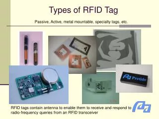
A Passive UHF RFID Tag IC. CLASS REPRESENTATION: Represented by: Khalil Monfaredi Advanced VLSI Course Seminar. Outline. Introduction to RFID (Radio Frequency Identification) Tag LSI (30%) Current Mode Rectifier (30%) Current Mode Demodulator (20%) FeRAM (10%) Summary (10%).

E N D
A Passive UHF RFID Tag IC CLASS REPRESENTATION: Represented by: Khalil Monfaredi Advanced VLSI Course Seminar
Outline • Introduction to RFID (Radio Frequency Identification) Tag LSI (30%) • Current Mode Rectifier (30%) • Current Mode Demodulator (20%) • FeRAM (10%) • Summary (10%)
RFID: Ubiquitous Sensing Networks Security Health care Thermometer Infrared Acceleration Danger • The present Person-to-person networking • The future Thing-to-thing networking • Thing-to-thing networking will begin • Sensing tags will play an important role
Requirements • Communication distance Long distance (10 m) • Incorporation of sensor device Transmit not only ID but also sensing data • Necessity of battery Battery life: as long as possible • Low cost
Comparison of Tags • Limited battery life: Solves by wireless power transmission
Required conversion efficiency Base station CW CW Tag Standby Recharge Downlink Uplink Time=1s Time=3ms Supply energy =40Ws Consume energy=0.3Ws Conversion efficiency > 0.75 %
Issues concerning rectifier CMOS rectifier DCcurrent RFin=40W Threshold voltage Vth Vin=0.2V Vin Vth 0 Zin |Zin|=700Vin=0.2V Region that cannot be rectified [2] • Cannot be rectified below threshold voltage Vth. • Vth=0V: There is a possibility that off-leak will occur.
Proposed rectifier • Apply a bias voltage Vbth Vth - Generating voltage of Vbth in the same IC chip DC+ = 0.3V @RFin=0.2V Vbth-Vth0 (S) M1 (G) 0.2V RFin Vbth RFin Vbth (D) Vth 0 M2 Vbth Region that cannot be rectified [2]
Vbth Vbth Vbth Vbth Stacked configuration • Stack 6 units of rectifiers to obtain over 1.5V DC DC+ Output DC voltage Vbth RFin Stack 6 units >1.5V Vbth 0.3V DC- [2] • How will 12 Vbth voltage sources be realized?
Realization of proposed rectifier INV1 INV2 High Low Vbth distributor PLS DC+ Vbth Cb1 VDD Cb2 6 units stacked Vbth=Vth Cb3 RFin Vbth generator Cb4 Vbth distributor [2] DC-
Realization of proposed rectifier INV1 INV2 Low High Vbth distributor PLS DC+ Vbth Cb1 Cb2 6 units stacked Vbth Cb3 RFin Cb4 Vbth Vbth distributor [2] DC-
Conventional NMOS Half-wave Rectifier Parasitic capacitance CP : Large Vth drop : External cancellation CP2 Vbth : External Vbth DC+ IN Mn2 CP3 CP Vbth Mn1 [2] DC -
Ferro cap. Proposed CMOS Half-wave Rectifier Parasitic capacitance CP : Small Vth drop : Internal cancellation DC+ PMOS CINF Cb IN CP Mp1 Mn1 Cb [1] DC - IVC (Internal Vth cancellation)
Proposed CMOS Full-wave Rectifier Circuit Good configuration for high efficiency IN+ D1 CINF VDD Over current IVC IVC IN - Over-current protection (AC GND) CP IVC IVC VSS D2 [1]
I IN VIN, Tag IC Prec Modulation index : (15%) Voltage Detection for Demodulator Near VIN VIN Device breakdown (4V) Small Far IIN Tag input Large Operating region Detection result Incoming Power Prec Time [1] Far Near
Current Detection for Demodulator Near IIN IIN Device breakdown (4V) I IN VIN, Large Tag IC VIN IIN Far Prec Tag input Large Operating region Detection result Modulation index : (15%) Incoming Power Prec Time [1] Far Near
Current-mode Demodulator Block Diagram ISIG = (IPK – IASK) IREF = IPK x n IPK IASK Modulated current (baseband) ISIG IASK LPF Subtraction + VASK Reference Current Generator IREF IPK Current comparator [1] Current Peak Hold
[3] [3]
[3] [3]
[3] [3]
FeRAM Adopted from ISSCC 2006 and also Stefano Bonetti, Johan Dahlbäck, Hanna Henricsson and Jutta Müntjes 26th of October 2005 2B1750 Smart Electonic Materials, KTH
Binary state 0 Positive electric field Positive polarization Binary state 1 Negative electric field Negative polarization FeRAM - Theory • Spontaneous polarization: above the Curie-temperature TC is the structure cubic, below a dipole moment occurs (displacement) • A different charge ΔQ can be observed whether the material is switching or non-switching: Example: PZT (lead zirconate-titanate) [4]
WL [4] WL WL PL PL PL BL’ BL BL Vref Sense AMP Sense AMP
Offset cell [4]
FeRAM - Requirements • Small size • High speed • High lifetime • Destructive reading (after every reading operation is a writing operation required) • Low coercive field • Low power memory devices • Large hysteresis • High remanent polarization
BL XBL WL SG CG AG PL BL FeRAM Characteristics High speed Low power [1]
Advantages of the Tag with FeRAM Condition : Read/Write operations Operating time Throughput Read 3.6ms Write 19.4ms 44tags/s EEPROM 2.9 times higher 66% reduction Read 3.6ms Write 4.2ms FeRAM 129tags/s [1]
Summary Passive UHF Read/Write Tag IC with FeRAM 4.3m Read/Write communication distance CMOS only rectifier which has 36.6% efficiency, 2.1 times higher than the conventional Low-voltage current-mode demodulator which has 27dB dynamic range for the incoming power Fabricated in 0.35-µm CMOS/FeRAM technology Tag throughput with FeRAM 2.9 times higher than tags with EEPROM for both read and write operations
References: [1] H. Nakamoto et al., “A Passive UHF RFID Tag LSI with 36.6% Efficiency CMOS-Only Rectifier and Current-Mode Demodulator in 0.35μm FeRAM Technology,” ISSCC Dig. Tech. Papers, session 17, 2006. [2] T. Umeda et al., “A 950MHz Rectifier Circuit for Sensor Networks with 10m-Distance,” ISSCC Dig. Tech. Papers, pp. 256-257, Feb., 2005. [3] A. Djemouai And M. Sawan., “New Cmos Current-mode Amplitude Shift Keying Demodulator (Askd) Dedicated For Implantable Electronic Devices,” IEEE (ISCAS), pp. 441-444, 2004. [4] S. Bonetti et al., “FeRAM, MRAM, RRAM ,” [online resource] Oct., 2005.