Download
1 / 21
300 likes | 659 Views
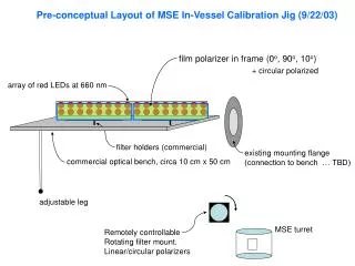
KGD Probing of TSVs at 40 um Array Pitch . 3D-TSV Probe Technology Goals MEMS probe tip evolution Contact performance TSV pad damage (or lack thereof) Conclusions. Ken Smith, Peter Hanaway, Mike Jolley, Reed Gleason, Chris Fournier, and Eric Strid. 3D-TSV Probe Technology Development Goals.

E N D
KGD Probing of TSVs at 40 um Array Pitch • 3D-TSV Probe Technology Goals • MEMS probe tip evolution • Contact performance • TSV pad damage (or lack thereof) • Conclusions Ken Smith, Peter Hanaway, Mike Jolley, Reed Gleason, Chris Fournier, and Eric Strid
3D-TSV Probe Technology Development Goals • Scale array pitch to 40 um • Reduce pad damage to allow prebond probe • Decrease cost of test • Simplified, high yield process • Fundamental understanding and accurate models of contact performance
RF filters, switches Process monitors (including M1 copper) RFSOC Multi-DUT Pyramid Probe Technology
3D Probing Requires a New Cost Structure Technology must be printed, repairable, scalable, compliant Constant cost per area DRAM & Flash Vertical probe: cost increases with density Logic/SoC 4 2 3D Requires constant cost per chip COGS/ pin ($) in 2012 1 Printed probe: nearly constant cost per area 0.50 0.25 0.12 Array Pitch (um) 0.06 3 6 1600 400 800 12 25 50 100 200
Scaling a Probe Card • Decrease XYZ dimensions by K • Same materials • Decrease Z motions by K • Force per tip decreases by K2; tip pressure constant 100 um pitch ~10 gm/tip 35 um pitch ~1 gm/tip
Wafer 3D TSV Probe Card Architecture • Pyramid Probe ST: Pads on membrane • Routing limitation ~3-4 rows deep from DUT pad perimeter • Replaceable contact layer PCB PCB Plunger
Replaceable Contact Layer • Tips are 5 um square and 20 um tall • 35 um pitch array • 24 x 48 tips
Contact resistance versus probing force • Single 12 um square tip • Sn plated wafer 5 um thick
Contact resistance versus probing force • 6 um tip • Force required is similar to 12 um tip
Force (gm•f ) vs. Deflection (um) • 1gm•f /um tip design • High durometer elastomer
Force (gm•f ) vs. Deflection (um) • 0.1 gm•f tip design • Low durometer elastomer
Pyramid Probe ST Routing • Unique fine-pitch routing • High-frequency performance similar to Pyramid Probes • Example is memory array • – 50 um x 40 um pad pitch • – 40 x 6 pad array
Optical photograph of probe mark array • Marks are exceptionally uniform • ~1 gram / contact for low pad damage
Profilometer scan of probe mark array • Maximum depth 100 nm • Maximum berm 500 nm
Probe marks on ENIG TSV pad • Exaggerated conditions: 10 TDs at 2.5 gf • Navigation grid (50 x 40 um) shows 3 probe marks on the 100 um diameter pad
Probe mark on ENIG pad • ~3 x 7 um • Exposed Ni ~50% • Depends on surface grains
Probe mark uniformity: Profilometer scans • Depth: Mean 68, Stdev 11 • Berm: Mean 363, Stdev 76
TDR traces on open and short • <40 ps rise / fall times (100 ps / div) • Limited by routing density in ST
Conclusions • Practical probe cards are capable of 40 um pitch and tip forces below 1 gm • Pad damage at these low forces is extremely small with scrub marks less than 100 nm deep • Lithographically printed probe cards enable a scalability path to lower cost and finer pitches • Probing the TSVs is not out of the question