Download
1 / 28
280 likes | 459 Views
CIRCUITI ELETTRONICI ANALOGICI E DIGITALI. LEZIONE N° 5 (3 ore) Inverter a BJT Caratteristica di trasferimento Inverter ideale Margini di rumore Fan-in e Fan-out Tempi di ritardo Dissipazione di potenza. Richiami. Giunzione p-n Circuiti equivalenti Logica a diodi e resistenze

E N D
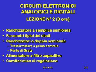
CIRCUITI ELETTRONICI ANALOGICI E DIGITALI LEZIONE N° 5 (3 ore) • Inverter a BJT • Caratteristica di trasferimento • Inverter ideale • Margini di rumore • Fan-in e Fan-out • Tempi di ritardo • Dissipazione di potenza C.E.A.D.
Richiami • Giunzione p-n • Circuiti equivalenti • Logica a diodi e resistenze • Limiti della logica a diodi e resistenze • Transistore bipolare (BJT) • Caratteristiche d’ingresso e d’uscita • Circuiti equivalenti C.E.A.D.
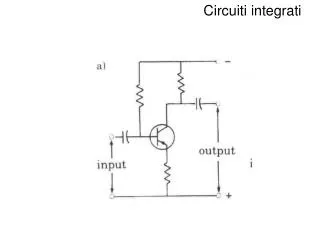
Inverter a BJT VBB = 0 ÷ 5 V VCC = 5 V RB = 200 KW RC = 5 KW (b = 200) RC VU RB VCC VBB C.E.A.D.
Passo A • VBB < 0.7 VEquazioni RC VU RB VCC VBB C.E.A.D.
Passo B • VBB > 0.7 V • Vero per Vu > 0.2 V RC RB VCC VU VBB bIB Vg C.E.A.D.
Passo C • VBB > 1.66 V RC RB VCC VU VBB VCESAT Vg C.E.A.D.
Caratteristica ingresso- uscita Interdizione VU A 5 B Lineare C Saturazione 0.2 0 VI 0.7 1.66 5 C.E.A.D.
Inverter ideale VU A INV 5 VI VU B 0 VI 5 2.5 C.E.A.D.
Inverter Reale • Ingresso • 0 logico • VI < 0.7 V • 1 logico • VI > 1.66 V • Uscita • 0 logico • Vu = 0.2 V • 1 logico • VI = 5 V Interdizione VU A 5 B Lineare C Saturazione 0.2 0 VI 0.7 1.66 5 C.E.A.D.
Margini di rumore 1 • Caratteristica generica VU 5 0 VI 5 C.E.A.D.
Margini di rumore 2 • Quesito • Dati due inverter in cascata, quali valori deve assumere l’uscita del primo affinché il secondo interpreti “giustamente” l’ingresso? VOH VIH VIL VOL C.E.A.D.
Determinazione dei margini • Punto della caratteristica dove è VU 5 VOH VOL 0 VIL VIH VI 5 C.E.A.D.
Margini di rumore 3 • Inverter Ideale • VIL = VIH = 2.5 V • VOL = 0 V • VOH = 5 V • NML = NMH = 2.5 V VU VOH VOL 0 VI VIL =VOH 5 C.E.A.D.
Margini di rumore 4 • Inverter Reale • VIL = 0.7 V • VIH = 1.66 V • VOL = 0.2 V • VOH = 5 V • NML = 0.7 - 0.2 = 0.5 V • NMH = 5 - 1.66 = 3.34 V VU A 5 B C 0.2 0 VI 0.7 1.66 5 C.E.A.D.
Margini di rumore 5 • Osservazione • Il minore fra NML e NMH condiziona il funzionamento della porta logica • Trigger di Smith NML > VDD/2 NMH > VDD/2 VOH VOL VIL VIH C.E.A.D.
Effetto caricante Valore minimo di VU = 4.5 V VCC = 5 V (b = 200) RB = 200 KWRC = 5 KW VCC RC RB VU VBB C.E.A.D.
Definizione • FAN-OUT • Numero max di ingressi elementari che un’uscita può pilotare • FAN-IN • Numero di ingressi elementari equivalenti che confluiscono su un ped d’ingresso C.E.A.D.
Inverter a BJT in commutazione VI VCC t IC 1 0.9 IC RC RB 0.1 VU 1 t VU 0.9 VI + - 0.1 td tr ts tf t ton toff C.E.A.D.
Osservazioni • td => delay time • tempo necessario a caricare la capacità base – emettitore e portare Ib al 10% del valore max • tr => rise time • tempo necessario a passare dal 10% al 90% del valore max (comportamento quasi lineare del BJT) • ts => storage time • tempo necessario a svuotare la base dalle cariche minoritarie immagazzinate nella condizione di saturazione • tf => fall time • tempo necessario a passare dal 90% al 10% del valore max (comportamento quasi lineare del BJT) • ton = td + tr toff = ts + tf C.E.A.D.
Ritardo in zona lineare • Per tr e tf il transistore è in zona lineare Rs rbb’ cc gm vb’e + - RC rb’e Vi ce tf = tr = µ t C.E.A.D.
Tempo di ciclo • Tciclo = tpLH + tpHL • fMAX = 1/ Tciclo VU 1 0.5 t 1 tpLH tpHL C.E.A.D.
Dissipazione di potenza • In generale è • Icoff > 0 , Vuon > 0 • c’è dissipazione statica • la massima dissipazione si ha durante la commutazione IC 1 0.9 0.1 VU 1 t 0.9 0.1 td tr ts tf t ton toff C.E.A.D.
Dissipazione di potenza • Dissipazione statica (uscita costante) • Dissipazione dinamica • Durante la commutazione si ha dissipazione C.E.A.D.
Osservazioni • La dissipazione statica può essere nulla • la dissipazione dinamica è di gran lunga la più importante • parametro di merito di una FAMIGLIA LOGICA • PRODOTTO RITARDO – CONSUMO • n.b. Frequentemente vengono forniti i due parametri separatamente C.E.A.D.
Dissipazione dell’inverter pd t IC 1 VU t Assumendo t0 = T1 (T2) 5 t t t T1 T2 C.E.A.D.
Esempio VBB = 0 ÷ 5 V VCC = 5 V RB = 500 KW RC = 5 KW (b = 200) CC = 5 pF FT = 200 MHz rb’e = 5 KW IC RC VU RB VCC Vin + - C.E.A.D.
Determinazione di t e Pd • Da 8.5 • Energia dissipata per commutazione e Pd C.E.A.D.
Conclusioni • Inverter a BJT • Caratteristica di trasferimento • Inverter ideale • Margini di rumore • Fan-in e Fan-out • Tempi di ritardo • Dissipazione di potenza C.E.A.D.