Download
1 / 29
300 likes | 526 Views
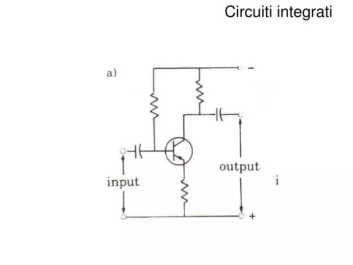
Circuiti integrati. Circuiti integrati. Circuiti integrati. Circuiti integrati. Circuiti integrati. Small-Scale Integration ( SSI ), <100 transistors 1960-1965 Medium-Scale Integration ( MSI ).100-3000 transistors 1965-1975

E N D
Circuiti integrati Small-Scale Integration (SSI), <100 transistors 1960-1965 Medium-Scale Integration (MSI).100-3000 transistors 1965-1975 Large-Scale Integration (LSI) 3000-100000 transistors 1975- 1980 Very -LSI (VLSI) 100000-1000000 1980-2000 Ultra -LSI (ULSI) more than 1 million transistors. Wafer Scale Integration (WSI) entire silicon wafer for a single "super-chip". Three Dimensional IC(3D-IC) has two or more layers of active electronic components that are integrated both vertically and horizontally into a single circuit.
First IC Computer 2 Kbytes RAM 36 Kbytes ROM
Jack Kilby with his lab notebook open at his first solid circuit drawing
Pentium 3 9.5 MTransistors
Deposito di SiO2, Si3N4, polysilicon Plasma enhanced chemical vapor deposition (PECVD) • Vantaggi Plasma: • Formazione radicali • Bombardamento ionico che • Produce rimozione e planarizzazione.
Deposito di metalli (sputtering) Physical Vapor Deposition (PVD)
Drogaggio per diffusione Figure 3.1-4: Intrinsic diffusion coefficients for the most common diffusers in silicon.
Drogaggio per impiantazione Channeling Fig. 2.2: Comparison of measured (SIMS) (black) and simulated (red) depth distribution profiles of 5 keV As ions implanted in Si at different implantation fluences under <100> channeling orientation. Long penetrating tails due to channeling, evident in the experimental profiles, are reproduced with very good accuracy by MC-BCA simulation
Drogaggio per impiantazione Damage
Drogaggio per impiantazione Annealing Figure 1 - Schematic of the ion implantation and pulsed-laser melting (II-PLM) process used by our group to synthesize semiconductor alloy films. A semiconductor wafer is first implanted with the alloying species and then irradiated with a single pulse from an excimer laser. The laser energy is converted to heat, which melts through the implant-damaged layer into the underlying substrate. Epitaxial solidification proceeds as heat is extracted into the substrate, resulting in a single-crystalline alloy film on the original substrate.