Download
1 / 1
10 likes | 136 Views
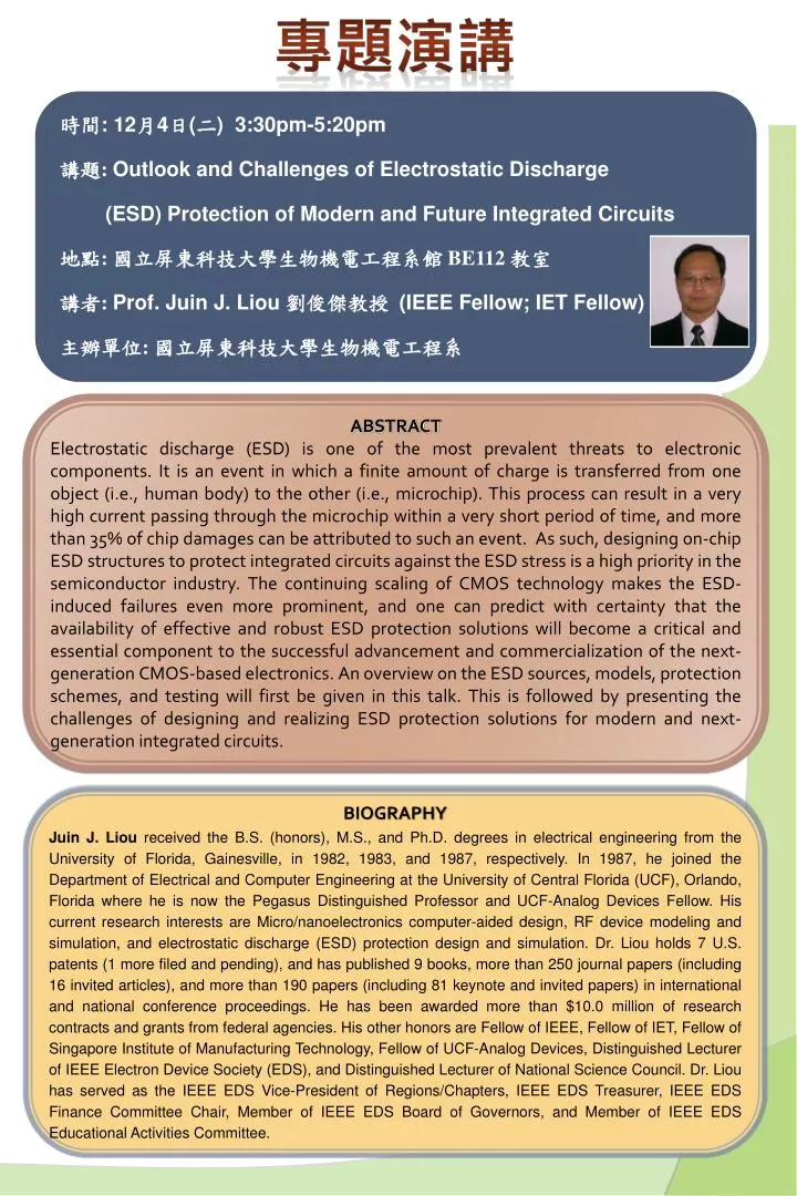
專題演講. 時間 : 12 月 4 日 ( 二 ) 3:30pm-5:20pm 講題 : Outlook and Challenges of Electrostatic Discharge (ESD) Protection of Modern and Future Integrated Circuits 地點 : 國立屏東科技大學生物機電工程系館 BE112 教室 講者 : Prof. Juin J. Liou 劉俊傑教授 (IEEE Fellow; IET Fellow) 主辦單位 : 國立屏東科技大學生物機電工程系. ABSTRACT

E N D
專題演講 時間:12月4日(二)3:30pm-5:20pm 講題:Outlook and Challenges of Electrostatic Discharge (ESD) Protection of Modern and Future Integrated Circuits 地點: 國立屏東科技大學生物機電工程系館 BE112 教室 講者:Prof. Juin J. Liou 劉俊傑教授 (IEEE Fellow; IET Fellow) 主辦單位: 國立屏東科技大學生物機電工程系 ABSTRACT Electrostatic discharge (ESD) is one of the most prevalent threats to electronic components. It is an event in which a finite amount of charge is transferred from one object (i.e., human body) to the other (i.e., microchip). This process can result in a very high current passing through the microchip within a very short period of time, and more than 35% of chip damages can be attributed to such an event. As such, designing on-chip ESD structures to protect integrated circuits against the ESD stress is a high priority in the semiconductor industry. The continuing scaling of CMOS technology makes the ESD-induced failures even more prominent, and one can predict with certainty that the availability of effective and robust ESD protection solutions will become a critical and essential component to the successful advancement and commercialization of the next-generation CMOS-based electronics.An overview on the ESD sources, models, protection schemes, and testing will first be given in this talk. This is followed by presenting the challenges of designing and realizing ESD protection solutions for modern and next-generation integrated circuits. BIOGRAPHY Juin J. Liou received the B.S. (honors), M.S., and Ph.D. degrees in electrical engineering from the University of Florida, Gainesville, in 1982, 1983, and 1987, respectively. In 1987, he joined the Department of Electrical and Computer Engineering at the University of Central Florida (UCF), Orlando, Florida where he is now the Pegasus Distinguished Professor and UCF-Analog Devices Fellow. His current research interests are Micro/nanoelectronics computer-aided design, RF device modeling and simulation, and electrostatic discharge (ESD) protection design and simulation. Dr. Liou holds 7 U.S. patents (1 more filed and pending), and has published 9 books, more than 250 journal papers (including 16 invited articles), and more than 190 papers (including 81 keynote and invited papers) in international and national conference proceedings. He has been awarded more than $10.0 million of research contracts and grants from federal agencies. His other honors are Fellow of IEEE, Fellow of IET, Fellow of Singapore Institute of Manufacturing Technology, Fellow of UCF-Analog Devices, Distinguished Lecturer of IEEE Electron Device Society (EDS), and Distinguished Lecturer of National Science Council. Dr. Liou has served as the IEEE EDS Vice-President of Regions/Chapters, IEEE EDS Treasurer, IEEE EDS Finance Committee Chair, Member of IEEE EDS Board of Governors, and Member of IEEE EDS Educational Activities Committee.