Download
1 / 13
130 likes | 219 Views
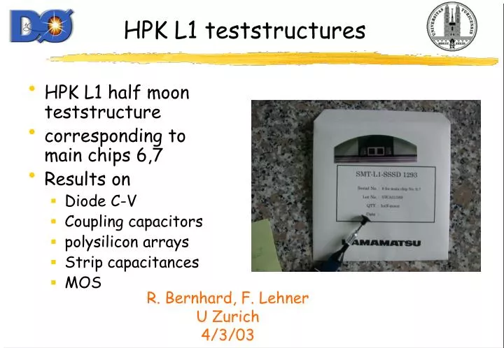
HPK L1 teststructures. HPK L1 half moon teststructure corresponding to main chips 6,7 Results on Diode C-V Coupling capacitors polysilicon arrays Strip capacitances MOS. R. Bernhard, F. Lehner U Zurich 4/3/03. HPK L1 teststructures. depletion voltage of diode ~110V

E N D
HPK L1 teststructures • HPK L1 half moon teststructure • corresponding to main chips 6,7 • Results on • Diode C-V • Coupling capacitors • polysilicon arrays • Strip capacitances • MOS R. Bernhard, F. Lehner U Zurich 4/3/03
HPK L1 teststructures • depletion voltage of diode ~110V • Corresponding sensor (HPK-L1 #6,7) depletion voltages: • 150V (HPK) • 130V (KSU), 110V (FNAL) • N.B. depletion voltage of segmented strip detector is ~5-10% higher than planar diode
HPK L1 teststructures • coupling capacitor test structure • same length than on sensor: 7.74 cm • low frequency limit: 115 pF => 14.8 pF/cm (in specs)
HPK L1 teststructures • CC breakdown ~220-230 V • similar to HPK-L2
HPK L1 teststructures • Aluminum trace teststructure (meander-like) • length 60 mm • resistance: 35 Ohm/cm (spec: 30 Ohm/cm) • HPK-L2: 16 Ohm/cm, smaller due to wider Al traces
HPK L1 teststructures • p+ implant structure • 130 kOhm/cm (on HPK-L2: 104 kOhm/cm)
HPK L1 teststructures • numerous polyresistor structures • different arrays: PS0, PS10, PS20, PS30 and PSH0 – PSH30 • What is the difference? • polysilicon material? • Processing? • doping?
HPK L1 teststructures • linearity from in range from –5V to +5V given for PS-30 and PS-20 resistor array • PS-10 and PS-0 have breakdown at ±2V • in linear region all resistors measured to be 1.05 ± 0.01 Mohm
HPK L1 teststructures • Baby detector w/ polysilicon resistors • R_poly: 0.7 ± 10% Mohm • R_poly + R_implant: • 1.5 ± 10% Mohm • implant alone: 130kOhm/cm • 1MOhm implant for 7.7 cm strip • not fully consistent !
HPK L1 teststructure • exact resistance value is difficult to measure, currents are low • value is irrelevant though, as long as R_inter >> R_poly • R_inter on babydetector ~ 10 Gohm (?)
HPK L1 teststructures • total strip capacitance • includes both neighbors • plus backplane capacitance • capacitance reaches plateau at ~10V • frequency dependence: Capacitance at 1 MHz: ~8.5pF Cap/cm: ~1.1 pF/cm
HPK L1 teststructures • interstrip capacitance • to one neighbor: ~3 pF => 0.39 pF/cm • to both neighbors: ~5.5 pF => 0.71 pF/cm
MOS structure • MOS (metal-oxide- silicon) structure • measure flatband voltage • use only 0.1V oscillator amplitude on LCR • high frequency (200kHz) • flatband shift to negative values? • interpretation not yet clear