Download
1 / 50
900 likes | 3.67k Views
Chapter 5: Imperfections in Solids. Imperfections in Solids. The properties of some materials are profoundly influenced by the presence of imperfections .

E N D
Imperfections in Solids • The properties of some materials are profoundly influenced by the presence of imperfections. • It is important to have knowledge about the types of imperfections that exist and the roles they play in affecting the behavior of materials.
Atom Purity and Crystal Perfection • If we assume a perfect crystal structure containing pure elements, then anything that deviated from this concept or intruded in this uniform homogeneity would be an imperfection. • There are no perfect crystals. • Many material properties are improved by the presence of imperfections and deliberately modified (alloying and doping).
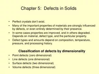
Types of Imperfections Line defects 1-dimensional • Dislocations Area defects 2-dimensional • Grain Boundaries • Vacancy atoms • Interstitial atoms • Substitutional atoms Point defects 1-2 atoms
Point Defects in Metals Vacancy distortion of planes self-interstitial distortion of planes • Vacancies: -vacant atomic sites in a structure. • Self-Interstitials: -"extra" atoms positioned between atomic sites.
Self Interstitials c05f01 • In metals, a self interstitial introduces relatively large distortions (strain) in the surrounding lattice since the atom is substantially larger than the interstitial site.
Point Defects in Ceramics Cation Interstitial Cation Vacancy Anion Vacancy • Vacancies -- vacancies exist in ceramics for both cations and anions • Interstitials -- interstitials exist for cations -- interstitials are not normally observed for anions because anions are large relative to the interstitial sites Adapted from Fig. 5.2, Callister & Rethwisch 3e. (Fig. 5.2 is from W.G. Moffatt, G.W. Pearsall, and J. Wulff, The Structure and Properties of Materials, Vol. 1, Structure, John Wiley and Sons, Inc., p. 78.)
Point Defects: Frenkel and Schottky Schottky Defect Frenkel Defect • Frenkel Defect To maintain the charge neutrality, a cation vacancy-cation interstitial pair occur together. The cation leaves its normal position and moves to the interstitial site. • Schottky Defect To maintain the charge neutrality, remove 1 cation and 1 anion; this creates 2 vacancies. Adapted from Fig. 5.3, Callister & Rethwisch 3e. (Fig. 5.3 is from W.G. Moffatt, G.W. Pearsall, and J. Wulff, The Structure and Properties of Materials, Vol. 1, Structure, John Wiley and Sons, Inc., p. 78.)
Equilibrium Concentration:Point Defects • Equilibrium concentration varies with temperature. Activation energy – energy required for formation of vacancy No. of defects æ ö N Q ç ÷ v v = ç ÷ exp No. of potential è ø N k T defect sites Temperature Boltzmann's constant -23 (1.38 x 10 J/atom-K) -5 (8.62 x 10 eV/atom-K) Each lattice site is a potential vacancy site
Measuring Activation Energy æ ö - N Q ç ÷ v v ç ÷ exp = è ø N k T • Measure this... • Replot it... slope N N v v ln N N - Q /k v exponential dependence! T 1/ T defect concentration • We can get Qv from an experiment.
Estimating Vacancy Concentration 0.9 eV/atom æ ö - N Q ç ÷ v v = ç ÷ exp = 2.7 x 10⁻⁴ è ø N k T 1273 K 8.62 x 10⁻⁵ eV/atom-K N A r x 1 m3 = 8.0 x 1028 sites x For 1 m3 , N = A Cu • Answer: N = (2.7 x 10⁻⁴)(8.0 x 1028) sites = 2.2 x 1025 vacancies v • Find the equil. # of vacancies in 1 m3 of Cu at 1000C. • Ex 5.1 - Given: 3 r = 8.4 g / cm A = 63.5 g/mol Cu N = 6.02 x 10²³ atoms/mol Q = 0.9 eV/atom v A
Point Defects in Polymers • Defects due in part to chain packing errors and impurities such as chain ends and side chains Adapted from Fig. 5.7, Callister & Rethwisch 3e.
Alloying • Given a metal (with only 1 type of atom) refined to 99.9999% purity, there would still exist 1022 to 1023 impurity atoms in 1 cubic meter of material. • Most metals are alloys. Alloying is done to improve strength, corrosion resistance, ductility, lower melting T. • For example, sterling silver is an alloy of 92.5% silver, 7.5% copper. At room temperature, “pure” silver is highly corrosion resistant, but also very soft. The addition of copper improves the strength and maintains good corrosion behavior.
Solid Solution • The addition of impurity atoms to a metal results in the formation of a solid solution. • The solvent represents the element that is present in the greatest amount (the host atoms). For example, in Lab 8 (MSE 227) Precipitation Hardening of Aluminum, aluminum is the solvent and copper is the solute (present in minor concentration ). • Solid solutions form when the solute atoms (Cu) are added to the solvent (Al), assuming the crystal structure is maintained and no new structures are formed.
Solid Solution - continued • A solid solution is a homogenous composition throughout. • The impurity atoms (Cu) are randomly and uniformly dispersed within the solid. • The impurity defects in the solid solution are either substitutional or interstitial.
Imperfections in Metals What are the outcomes if impurity (B) is added to host (A)? • Solid solution of B in A (random distribution of point defects) OR Substitutional solid solution. (e.g., Cu in Ni) Interstitial solid solution. (e.g., C in Fe) • Solid solution of B in A plus particles of a new phase (usually for a larger amount of B) Second phase particle -- different composition -- often different structure.
Hume - Rothery Rules The Hume-Rothery rules are basic conditions for an element to dissolve in a metal, forming a substitutional solid solution. • The atomic radius of the solute and solvent atoms must differ by no more than 15% (r < 15%). • The solute and solvent should have similar electronegativities. • Same crystal structure for “pure” metals. • Maximum solubility occurs when the solvent and solute have the same valence. Metals with lower valence will tend to dissolve metals with higher valence.
Element Atomic Crystal Electro- Valence Radius Structure nega- (nm) tivity Cu 0.1278 FCC 1.9 +2 C 0.071 2.5 H 0.046 O 0.060 Ag 0.1445 FCC 1.9 +1 Al 0.1431 FCC 1.5 +3 Co 0.1253 HCP 1.8 +2 Cr 0.1249 BCC 1.6 +3 Fe 0.1241 BCC 1.8 +2Ni 0.1246 FCC 1.8 +2 Pd 0.1376 FCC 2.2 +2 Zn 0.1332 HCP 1.6 +2 Substitutional Solid Solution Example: Copper and Nickel
Interstitial Solid Solution • Carbon forms an interstitial solid solution when added to iron; the maximum concentration of carbon that can be added is roughly 2%. • The atomic radius of the carbon atom is much less than that of iron (0.071nm vs 0.124 nm). • For interstitial solid solutions, the Hume-Rothery rules are: • 1. Solute atoms must be smaller than the pores in the solvent lattice. • 2. The solute and solvent should have similar electronegativity.
Imperfections in Ceramics + - Na Cl cation vacancy 2+ Ca + Na + Na 2+ Ca 2+ without impurity Ca impurity with impurity • Substitutional anion impurity an ion vacancy 2- O - - Cl Cl 2- without impurity O impurity with impurity • • Since there are both anions and cations in ceramics, a substitutional impurity will replace the host ion most similar in terms of charge. • Charge balance must be maintained when impurities are present. • Ex: NaCl • Substitutional cation impurity
Point Defects: Impurities c05f06
Types of Imperfections Line defects 1-dimensional • Dislocations • Vacancy atoms • Interstitial atoms • Substitutional atoms Point defects 1-2 atoms 22
Line Defects Dislocations: • are line defects, • slip between crystal planes result when dislocations move, • produce permanent (plastic) deformation. Schematic of Zinc (HCP): • before deformation • after tensile elongation slip steps
Imperfections in Solids Linear defects (Dislocations) are one-dimensional defects that cause misalignment of nearby atoms. Linear defects are associated primarily with mechanical deformation. Types of dislocations: edge, screw, mixed. Edge dislocation: • extra half-plane of atoms inserted in a crystal structure; the edge of the plane terminates within the crystal. • Around the dislocation line there is some localized distortion. • b perpendicular () to dislocation line Burger’s vector, b: measure of lattice distortion 24
Motion of Edge Dislocation • • Dislocation motion requires the successive bumping • of a half plane of atoms (from left to right). • • Bonds across the slipping planes are broken and • remade in succession. • The (plastic) permanent deformation of most crystalline materials is by dislocation movement. • Most contain some dislocations that were introduced during solidification, plastic deformations, and rapid cooling (thermal stresses). • To deform plastically means to slide atomic planes past each other. Atomic view of edge dislocation motion from left to right as a crystal is sheared.
Dislocations • The strength of a material with no dislocations is 20-100 times greater than the strength of a material with a high dislocation density. • So, materials with no dislocations may be very strong, but they cannot be deformed. • The dislocations weaken a material, but make plastic deformation possible.
Imperfections in Solids Screw dislocation: • Named for the spiral stacking of crystal planes around the dislocation line; results from shear deformation • b parallel () to dislocation line
Dislocation Motion Plastically stretched zinc single crystal. • Produces plastic deformation, • Depends on incrementally breaking bonds. • If dislocations don't move, deformation doesn't happen!
Characteristics of Dislocations • During plastic deformation, the number of dislocations increase dramatically to densities of 1010 mm-2. • Grain boundaries, internal defects and surface irregularities serve as formation sites for dislocations during deformation.
Dislocations During Cold Working • Ti alloy after cold working. • Dislocations entangle with one another during cold work. • Dislocation movement becomes more difficult. • Dislocations are visible in electron micrographs
Types of Imperfections Line defects 1-dimensional • Dislocations • Vacancy atoms • Interstitial atoms • Substitutional atoms Point defects 1-2 atoms Area defects 2-dimensional • Grain Boundaries 32
Polycrystalline Materials Grain Boundaries • regions between crystals • transition from lattice of one region to another • The atoms near the boundaries of the 3 grains do not have an equilibrium spacing or arrangement; slightly disordered. • Grains and grain boundaries in a stainless steel sample. low density in grain boundaries
Planar Defects in Solids - Twinning • A shear force that causes atomic displacements such that the atoms on one side of a plane (twin boundary) mirror the atoms on the other side. A reflection of atom positions across the twin plane. • Displacement magnitude in the twin region is proportional to the atom’s distance from the twin plane. • Takes place along defined planes and directions depending upon the system. • Ex: BCC twinning occurs on the (112)[111] system
(c) 2003 Brooks/Cole Publishing / Thomson Learning Twinning Applied stress to a perfect crystal (a) may cause a displacement of the atoms, (b) causing the formation of a twin. Note that the crystal has deformed as a result of twinning. • Stacking faults • For FCC metals an error in ABCABC packing sequence • Ex: ABCABABC
Properties of Twinning • Of the three common crystal structures BCC, FCC and HCP, the HCP structure is the most likely to twin. • FCC structures will not usually twin because slip is more energetically favorable. • Twinning occurs at low temperatures and high rates of shear loading (shock loading) conditions where there are few present slip systems (restricting the possibility of slip) • Small amount of deformation when compared with slip.
Slip Systems • Usually there are preferred slip planes and directions in crystal systems. • The combination of both the slip plane and direction form the slip system. • Slip plane is generally taken as the closest packed plane in the system • Slip direction is taken as the direction on the slip plane with the highest linear density.
Slip systems • FCC and BCC materials have large numbers of slip systems (at least 12) and are considered ductile. • HCP systems have few slip systems and are quite brittle.
(c) 2003 Brooks/Cole Publishing / Thomson Learning A micrograph of twins within a grain of brass (x250).
Microscopic Examination • Metallography – sample preparation is necessary to examine the surface of materials (metals, ceramics, polymers). • A smooth mirror-like finish is obtained by grinding and polishing using successively finer abrasive papers and powder mixed with water. • The microstructure (grain size, shape, orientation) is revealed using a chemical reagent (etching solution) on a polycrystalline sample. • Etching characteristics vary from grain to grain.
Optical Microscopy 0.75mm • Useful up to 2000X magnification. • Polishing removes surface features (e.g., scratches) • Etching changes reflectance, depending on crystal orientation. crystallographic planes Micrograph of brass (a Cu-Zn alloy)
Optical Microscopy polished surface surface groove grain boundary (a) ASTM grain size number n -1 N = 2 number of grains/in2 Fe-Cr alloy at 100x (b) magnification Grain boundaries... • are imperfections, • are more susceptible to etching, • may be revealed as dark lines, • change in crystal orientation across boundary. Adapted from Fig. 5.19(a) and (b), Callister & Rethwisch 3e. (Fig. 5.19(b) is courtesy of L.C. Smith and C. Brady, the National Bureau of Standards, Washington, DC [now the National Institute of Standards and Technology, Gaithersburg, MD].)
Microscopy Optical (light) resolution (0.1 m = 100 nm = 10-7 m) For higher resolution need higher frequency • X-Rays are difficult to focus. • Electrons • wavelengths are roughly 3 pm (0.003 nm) • (Magnification - 1,000,000X) • Atomic resolution possible • Electron beam focused by magnetic lenses.