Download
1 / 13
210 likes | 797 Views
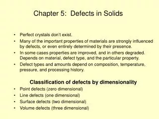
Chapter 5 Defects in solids. All solid materials… contain large # of defects. Solidification process…. above T m. classification. Defects… imperfection in structures of solid materials crystal structure due to irregular/disordered atomic arrangement.

E N D
All solid materials… • contain large # of defects. Solidification process… above Tm classification • Defects… • imperfection in structures of solid materials • crystal structure due to irregular/disordered atomic arrangement. • amorphous structure due to molecular chains error. - classify in terms of geometry (dimension) & size. • normally, formed during solidification process. zero dimension one dimension two dimension three dimension nuclei liquid Defects in solids Solidification process… • result of primary materials forming/working. • i.e: for metals, casting process. • 2 steps: • 1. Nuclei form – formation of stable nuclei. • 2. Nuclei grow to form crystals – formation of grain • structure. • start with a molten (all liquid) material & grains (crystals) grow until they meet each other. point defects Linear/dislocation defects area/planar/surface defects volume defects (i.e: crack) crystals growing crystal growing - Grains structure can be: 1. equiaxed grains (roughly same size in all directions). 2. columnar grains (elongated grains). room temp. grain structure Columnar grains in area with less undercooling Mold Equiaxed grains due to rapid cooling (greater T) near wall Casting process
Defects in solids Point defects in ceramics 1. Vacancies - vacancies exist in ceramics for both cations and anions. Cation 2. Interstitials - exist for cations only. - interstitials are not normally observed for anions because anions are large relative to the interstitial sites. Interstitial distortion distortion of planes 3. Frenkel defect - a cation vacancy-cation interstitial pair. Cation of planes Vacancy Anion 4. Schottky defect - a paired set of cation and anion vacancies. self-interstitial Vacancy Vacancy Schottky defect Frenkel defect 10 nm classification zero dimension point defects metals ceramics polymers Point defects in metals 2. Vacancies 1. Self-Interstitials • vacant atomic sites exist in a structure. • form due to a missing atom. • form (one in 10,000 atoms) during • crystallization, mobility of atoms or • rapid cooling. - "extra" atoms positioned between atomic sites. - cause structural distortion. interstitial, vacancy, Frenkel & Schottky, substitutional anion & cation impurity self-interstitial & vacancy (metals) interstitial & substitutional (metal alloys) Chain packing error Point defects in polymers • Defects due in part to chain packing errors and • impurities such as chain ends and side chains. • i.e: thin platelets Adapted from Fig. 4.12, Callister & Rethwisch 3e.
Defects in solids 0.9 eV/atom slope æ ö - ln N Q N ç ÷ v v N v = v ç ÷ exp - Q /k = 2.7 x 10⁻⁴ v è ø N k T N N 1273 K 1/ T 8.62 x 10⁻⁵ eV/atom-K N A r x 1 m3 = 8.0 x 1028 atom sites x For 1 m3 , N = A Cu = N ACu VCu NA N = (2.7 x 10⁻⁴)(8.0 x 1028) sites = 2.2 x 1025 vacancies v Measuring Activation Energy… Equilibrium concentration: Point defects • We can get Qv from an experiment. • equilibrium # of point defects (vacancies) for • solids depends on & increase with temperature. • apply the formula: classification • Measure this... zero dimension # of vacancy sites, Nv Vacancy concentration = total # of atomic sites, N point defects exponential æ ö dependence! N Q ç v v = ç exp è ø T N k T Defect (@ vacancy) concentration Nv = # of defects (vacancies site) • Replot it... N = total # of atomic sites T = temperature metals ceramics polymers Qv = activation energy k = Boltzmann's constant (1.38 x 10⁻²³ J/atom-K) (8.62 x 10⁻⁵ eV/atom-K) - each lattice/atom site is potential vacancy site. Answer: Example: interstitial, vacancy, Frenkel & Schottky, substitutional anion & cation impurity (a) self-interstitial & vacancy (pure metals) interstitial & substitutional (metals alloy) Chain packing error In 1 m3 of Cu at 1000C, calculate: (a) vacancy concentration, Nv/N. (b) equilibrium # of vacancies, Nv. Given that, r (b) = 8.4 g / cm3 Qv = 0.9 eV/atom ACu = 63.5 g/mol NA = 6.02 x 10²³ atoms/mol
Defects in solids General concept… • Metal alloys are used in most • engineering applications. • Metal alloy is a mixture of two or • more metals and nonmetals. • Solid solution is a simple type of • metal alloy in which elements are • dispersed in a single phase. + - Na Cl Impurities in ceramics • Electroneutrality (charge balance) must be • maintained when impurities are present. 2. Substitutional anion impurity classification 2- O i.e: NaCl zero dimension cation - - Cl Cl 1. Substitutional cation impurity point defects vacancy 2- without impurity O impurity 2+ Ca + Na an ion vacancy + Na 2+ Ca 2+ with impurity without impurity Ca impurity metals ceramics polymers with impurity Impurities in metals Two outcomes if impurity (B) added to host (A): 1. Small amount of B added to A interstitial, vacancy, Frenkel & Schottky, substitutional anion & cation impurity self-interstitial & vacancy (metals) interstitial & substitutional (metal alloys) Chain packing error Substitutional solid soln. (e.g., Cu in Ni) Interstitial solid soln. (e.g., C in Fe) 2. Large amount of B added to A plus particles of a new phase Second phase particle - different composition. - often different structure.
Defects in solids Impurities in metals • Conditions for solid solubility • - apply W. Hume – Rothery rule. • have 4 conditions which is applied for • substitutional solid solution. • The solubility of solids is greater if: • r(atomic radius difference) < 15%. • Proximity in periodic table • -- i.e, similar electronegativities. • Same crystal structure for pure metals. • Valency • -- all else being equal, a metal will • have a greater tendency to dissolve • another metal of higher valency than • one of lower valency. Example 1: • Specification of composition • determine the composition for a 2 • element in alloy system. • specify in weight percent, wt % @ • atom percent, at %. • Would you predict more Al or Ag to dissolve in Zn? • 2. More Zn or Al in Cu? Element Atomic Crystal Electro- Valence Radius (nm) Structure negativity Cu 0.1278 FCC 1.9 +2 C 0.071 H 0.046 O 0.060 Ag 0.1445 FCC 1.9 +1 Al 0.1431 FCC 1.5 +3 Co 0.1253 HCP 1.8 +2 Cr 0.1249 BCC 1.6 +3 Fe 0.1241 BCC 1.8 +2 Ni 0.1246 FCC 1.8 +2 Pd 0.1376 FCC 2.2 +2 Zn 0.1332 HCP 1.6 +2 • weight percent, wt% C2 = 100 – C1 m1 & m2 = mass of component 1 & 2 C1 & C2 = composition (in wt%) of component 1 & 2 • atom percent, at% C’2 = 100 – C’1 C1 = m1 x 100 C’1 = nm1 x 100 nm1 = m1/A1 nm2 = m2/A2 m1+ m2 nm1+ nm2 nm1 & nm2 = number of moles of component 1 & 2 A1 & A2 = at. weight of component 1 & 2 C’1 & C’2 = composition (in at%) of component 1 & 2 classification zero dimension point defects metals ceramics polymers Example 2: interstitial, vacancy, Frenkel & Schottky, substitutional anion & cation impurity self-interstitial & vacancy (metals) interstitial & substitutional (metal alloys) Chain packing error Lower solid solubility (interstitial S.S) Higher solid solubility (subs. S.S) Example 3: A hypothetical alloy consist of 120 g element A & 80 g element B. Determine the composition (in wt%) for each element?
Defects in solids Mixed Screw Dislocation Edge b (b) Dislocation line Burgers vector b (a) Screw Linear defects in materials SEM micrograph shows dislocation as a dark lines • also known as dislocations. • defects around which atoms are misaligned • in a line @ lattice distortions are centered • around a line. • slip between crystal planes result when disl. • moves. • formed during solidification @ permanent • deformation. classification Dislocations in Zinc (HCP) one dimension linear defects slip steps SEM micrograph Type of dislocations… 1. Edge dislocation: - extra half-plane of atoms inserted in a crystal structure. - b perpendicular to dislocation line. initial All materials after tensile elongation • 2. Screw dislocation: • spiral planar ramp resulting from shear • deformation. • - b parallel to dislocation line. edge dislocation screw dislocation mixed dislocation 3. Mixed dislocation: - most crystal have components of both edge and screw dislocation. Edge dislocation Screw dislocation Mixed dislocation
Dislocations & Crystal Structures • Structure: close-packed planes & directions are preferred. view onto two close-packed planes. close-packed directions close-packed plane (bottom) close-packed plane (top) • Comparison among crystal structures: FCC: many close-packed planes/directions; HCP: only one plane, 3 directions; BCC: none • Specimens that were tensile tested. Mg (HCP) Higher solid solubility (subs. S.S) tensile direction Al (FCC)
Defects in solids Grain boundaries in 1018 steel Twin plane Twin Planar defects in materials • Defects due to formation of grains structure. classification • 1. Grain boundaries • - region between grains (crystallites). • - formed due to simultaneously growing • crystals meeting each other. • - slightly disordered. • - restrict plastic flow and prevent dislocation • movement (control crystal slip). • - low density in grain boundaries -- high mobility. -- high diffusivity. -- high chemical reactivity. two dimension planar/surface defects All materials 2. Twin boundaries - essentially a reflection of atom positions across the twin plane. - a region in which mirror image of structure exists across a boundary. - formed during plastic deformation and recrystallization. - strengthens the metal. grain boundaries twin boundaries stacking faults 3. Stacking faults - piling up faults during recrystallization due to collapsing. - for FCC metals an error in ABCABC packing sequence, i.e: ABCABABC.
Catalysts and Surface Defects Catalyst is a substance in solid form. A catalyst increases the rate of a chemical reaction without being consumed. Reactant molecules in a gas @ liquid phase (CO, NOx & O2) are absorbed onto catalyst surface. Reduce the emission of exhaust gas pollutants. Adsorption/active sites on catalysts are normally surface defects. Fig. 5.15, Callister & Rethwisch 3e. Single crystals of (Ce0.5Zr0.5)O2used in an automotive catalytic converter Fig. 5.16, Callister & Rethwisch 3e.
Defects in solids Process flow… 1. mount 2. grind 3. polish 4. clean 5. etch 6. observe 7. analyze polished surface surface groove grain boundary Etched Brass 200 X Unetched Steel 200 X Etched Steel 200 X Unetched Brass 200 X Fe-Cr alloy 0.75mm Microscopic examination • such microscope used to observe & analyze • structures @ defects of materials. • i.e: OM, IM, SEM, TEM, STM, AFM etc. microscopic examination Grain boundaries observation • used metallographic techniques. • the metal sample must be first mounted for easy • handling. • - then the sample should be ground and polished • -- with different grades of abrasive paper and • abrasive solution. • -- removes surface features (e.g., scratches). • the surface is then etched chemically. • -- tiny groves are produced at grain boundaries. • -- groves do not intensely reflect light. • -- may be revealed as dark lines. • - hence observed by optical microscope. Inverted Microscope (IM) Transmission Electron Microscope (TEM) Scanning Tunneling Microscope (STM) Optical Microscope (OM) Scanning Electron Microscope (SEM) Atomic Force Microscope (AFM) metallographic techniques Effect of etching… SEM micrograph observe grain structure & boundaries analyze grain size examine topographical map (surface features) STM topographic
1045 cold rolled steel, n=8 1018 cold rolled steel, n=10 3 inches 5 grains • Size of grains… • - affects the mechanical properties of the material. • the smaller the grain size, more are the grain • boundaries. • more grain boundaries means higher resistance to • slip (plastic deformation occurs due to slip). • more grains means more uniform the mechanical • properties are. Defects in solids How to measure grain size? • use the formula: • N = 2n -1 microscopic examination n = ASTM grain size number. N = number of grains per square inch of a polished & etched specimen at 100x magnification. • ASTM grain size number ‘n’ is a • measure of grain size. Measuring average grain diameter • Average grain diameter, d more directly • represents grain size. • Random line of known length is drawn on • photomicrograph. • - Number of grains intersected is counted. • Ratio of number of grains intersected to length of • line, nL is determined. • d = C/nL(M) C = 1.5 & M = magnification n < 3 – Coarse grained 4 < n < 6 – Medium grained 7 < n < 9 – Fine grained n > 10 – ultrafine grained Inverted Microscope (IM) Transmission Electron Microscope (TEM) Scanning Tunneling Microscope (STM) Optical Microscope (OM) Scanning Electron Microscope (SEM) Atomic Force Microscope (AFM) - If ASTM grain size #, n increase, -- size of grains decrease. -- # of grains/in2, N increase. metallographic techniques observe grain structure & boundaries analyze grain size examine topographical map (surface features) Example: log N = (n-1) log 2 Determine the ASTM grain size number of a metal specimen if 45 grains per square inch are measured at a magnification of 100x. n = log N + 1 log 2 n = log 45 + 1 log 2 n = 6.5
Summary • Point, Line, and Area defects exist in solids. • The number and type of defects can be varied and controlled (e.g., T controls vacancy conc.) • Defects affect material properties (e.g., grain boundaries control crystal slip). • Defects may be desirable or undesirable (e.g., dislocations may be good or bad, depending on whether plastic deformation is desirable or not.)