Download
1 / 47
470 likes | 475 Views
This article explores the memory hierarchy in computer systems, focusing on cache design and tradeoffs. It discusses the different levels of caches, memory, and disks, as well as the principles of locality and the importance of caches. The article also covers direct-mapped caches, their properties, and design issues.

E N D
The Memory HierarchyCS 740Sept. 28, 2001 • Topics • The memory hierarchy • Cache design
Processor interrupts Cache Memory-I/O bus I/O controller I/O controller I/O controller Memory Display Network disk disk Disk Disk Computer System
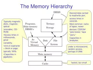
C a c h e C a c h e The Tradeoff cache virtual memory CPU Memory disk 16 B 8 B 4 KB regs register reference L1-cache reference L2-cache reference memory reference disk memory reference size: speed: $/Mbyte: block size: 608 B 1.4 ns 4 B 128k B 4.2 ns 4 B 512kB -- 4MB 16.8 ns $90/MB 16 B 128 MB 112 ns $2-6/MB 4-8 KB 27GB 9 ms $0.01/MB larger, slower, cheaper (Numbers are for a 21264 at 700MHz)
Why is bigger slower? • Physics slows us down • Racing the speed of light: (3.0x10^8m/s) • clock = 500MHz • how far can I go in a clock cycle? • (3.0x10^8 m/s) / (500x10^6 cycles/s) = 0.6m/cycle • For comparison: 21264 is about 17mm across • Capacitance: • long wires have more capacitance • either more powerful (bigger) transistors required, or slower • signal propagation speed proportional to capacitance • going “off chip” has an order of magnitude more capacitance
Alpha 21164 Chip Photo Microprocessor Report 9/12/94 • Caches: L1 data L1 instruction L2 unified + L3 off-chip
Alpha 21164 Chip Caches Right Half L2 L3 Control • Caches: L1 data L1 instruction L2 unified + L3 off-chip L1 Data L1 I n s t r. Right Half L2 L2 Tags
Locality of Reference • Principle of Locality: • Programs tend to reuse data and instructions near those they have used recently. • Temporal locality:recently referenced items are likely to be referenced in the near future. • Spatial locality:items with nearby addresses tend to be referenced close together in time. sum = 0; for (i = 0; i < n; i++) sum += a[i]; *v = sum; • Locality in Example: • Data • Reference array elements in succession (spatial) • Instructions • Reference instructions in sequence (spatial) • Cycle through loop repeatedly (temporal)
Big, Slow Memory A A B B G C H • • • Y Z Caching: The Basic Idea Small, Fast Cache • Main Memory • Stores words A–Z in example • Cache • Stores subset of the words 4 in example • Organized in lines • Multiple words • To exploit spatial locality • Access • Word must be in cache for processor to access Processor
How important are caches? • 21264 Floorplan • Register files in middle of execution units • 64k instr cache • 64k data cache • Caches take up a large fraction of the die (Figure from Jim Keller, Compaq Corp.)
b a Accessing Data in Memory Hierarchy • Between any two levels, memory is divided into lines (aka “blocks”) • Data moves between levels on demand, in line-sized chunks • Invisible to application programmer • Hardware responsible for cache operation • Upper-level lines a subset of lower-level lines Access word w in line a (hit) Access word v in line b (miss) w v High Level a a a b b Low Level b b a a
Design Issues for Caches • Key Questions: • Where should a line be placed in the cache? (line placement) • How is a line found in the cache? (line identification) • Which line should be replaced on a miss? (line replacement) • What happens on a write? (write strategy) • Constraints: • Design must be very simple • Hardware realization • All decision making within nanosecond time scale • Want to optimize performance for “typical” programs • Do extensive benchmarking and simulations • Many subtle engineering tradeoffs
Direct-Mapped Caches • Simplest Design • Each memory line has a unique cache location • Parameters • Line (aka block) size B = 2b • Number of bytes in each line • Typically 2X–8X word size • Number of Sets S = 2s • Number of lines cache can hold • Total Cache Size = B*S = 2b+s • Physical Address • Address used to reference main memory • n bits to reference N = 2n total bytes • Partition into fields • Offset: Lower b bits indicate which byte within line • Set: Next s bits indicate how to locate line within cache • Tag: Identifies this line when in cache n-bit Physical Address t s b tag set index offset
t s b tag set index offset Indexing into Direct-Mapped Cache Set 0: 0 1 • • • B–1 • Use set index bits to select cache set Tag Valid Set 1: 0 1 • • • B–1 Tag Valid • • • 0 1 • • • B–1 Set S–1: Tag Valid Physical Address
t s b tag set index offset Direct-Mapped Cache Tag Matching • Identifying Line • Must have tag match high order bits of address • Must have Valid = 1 = 1? Selected Set: = ? 0 1 • • • B–1 Tag Valid • Lower bits of address select byte or word within cache line Physical Address
Properties of Direct Mapped Caches • Strength • Minimal control hardware overhead • Simple design • (Relatively) easy to make fast • Weakness • Vulnerable to thrashing • Two heavily used lines have same cache index • Repeatedly evict one to make room for other Cache Line
Vector Product Example float dot_prod(float x[1024], y[1024]) { float sum = 0.0; int i; for (i = 0; i < 1024; i++) sum += x[i]*y[i]; return sum; } • Machine • DECStation 5000 • MIPS Processor with 64KB direct-mapped cache, 16 B line size • Performance • Good case: 24 cycles / element • Bad case: 66 cycles / element
Thrashing Example x[0] y[0] • Access one element from each array per iteration x[1] Cache Line y[1] Cache Line x[2] y[2] x[3] y[3] • • • • • • Cache Line Cache Line • • • • • • x[1020] y[1020] x[1021] Cache Line y[1021] Cache Line x[1022] y[1022] x[1023] y[1023]
Access Sequence Read x[0] x[0], x[1], x[2], x[3] loaded Read y[0] y[0], y[1], y[2], y[3] loaded Read x[1] Hit Read y[1] Hit • • • 2 misses / 8 reads Analysis x[i] and y[i] map to different cache lines Miss rate = 25% Two memory accesses / iteration On every 4th iteration have two misses Timing 10 cycle loop time 28 cycles / cache miss Average time / iteration = 10 + 0.25 * 2 * 28 Thrashing Example: Good Case x[0] y[0] x[1] y[1] Cache Line x[2] y[2] x[3] y[3]
Access Pattern Read x[0] x[0], x[1], x[2], x[3] loaded Read y[0] y[0], y[1], y[2], y[3] loaded Read x[1] x[0], x[1], x[2], x[3] loaded Read y[1] y[0], y[1], y[2], y[3] loaded • • • 8 misses / 8 reads Analysis x[i] and y[i] map to same cache lines Miss rate = 100% Two memory accesses / iteration On every iteration have two misses Timing 10 cycle loop time 28 cycles / cache miss Average time / iteration = 10 + 1.0 * 2 * 28 Thrashing Example: Bad Case x[0] y[0] x[1] y[1] Cache Line x[2] y[2] x[3] y[3]
0 0 0 1 1 1 • • • • • • • • • B–1 B–1 B–1 Tag Tag Tag Valid Valid Valid Set Associative Cache • Mapping of Memory Lines • Each set can hold E lines (usually E=2-8) • Given memory line can map to any entry within its given set • Eviction Policy • Which line gets kicked out when bring new line in • Commonly either “Least Recently Used” (LRU) or pseudo-random • LRU: least-recently accessed (read or written) line gets evicted LRU State Line 0: Set i: Line 1: • • • Line E–1:
0 0 0 0 0 0 1 1 1 1 1 1 • • • • • • • • • • • • • • • • • • B–1 B–1 B–1 B–1 B–1 B–1 Tag Tag Tag Tag Tag Tag Valid Valid Valid Valid Valid Valid t s b tag set index offset Indexing into 2-Way Associative Cache • Use middle s bits to select from among S = 2s sets Set 0: Set 1: • • • Set S–1: Physical Address
0 0 1 1 • • • • • • B–1 B–1 Tag Tag Valid Valid t s b tag set index offset Associative Cache Tag Matching • Identifying Line • Must have one of the tags match high order bits of address • Must have Valid = 1 for this line = 1? Selected Set: = ? • Lower bits of address select byte or word within cache line Physical Address
Cache Data Cache Tag Valid Cache Line 0 : : : Compare Two-Way Set Associative CacheImplementation • Set index selects a set from the cache • The two tags in the set are compared in parallel • Data is selected based on the tag result Set Index Valid Cache Tag Cache Data Cache Line 0 : : : Adr Tag Adr Tag Compare 1 0 Mux Sel1 Sel0 OR Cache Line Hit
0 0 0 1 1 1 • • • • • • • • • B–1 B–1 B–1 Tag Tag Tag Valid Valid Valid Fully Associative Cache • Mapping of Memory Lines • Cache consists of single set holding E lines • Given memory line can map to any line in set • Only practical for small caches Entire Cache LRU State Line 0: Line 1: • • • Line E–1:
0 0 0 1 1 1 • • • • • • • • • B–1 B–1 B–1 Tag Tag Tag Valid Valid Valid Fully Associative Cache Tag Matching = 1? • Identifying Line • Must check all of the tags for match • Must have Valid = 1 for this line • • • • • • = ? • Lower bits of address select byte or word within cache line t b tag offset Physical Address
Replacement Algorithms • When a block is fetched, which block in the target set should be replaced? • Optimal algorithm: • replace the block that will not be used for the longest period of time • must know the future • Usage based algorithms: • Least recently used (LRU) • replace the block that has been referenced least recently • hard to implement • Non-usage based algorithms: • First-in First-out (FIFO) • treat the set as a circular queue, replace block at head of queue. • easy to implement • Random (RAND) • replace a random block in the set • even easier to implement
Implementing RAND and FIFO • FIFO: • maintain a modulo E counter for each set. • counter in each set points to next block for replacement. • increment counter with each replacement. • RAND: • maintain a single modulo E counter. • counter points to next block for replacement in any set. • increment counter according to some schedule: • each clock cycle, • each memory reference, or • each replacement anywhere in the cache. • LRU • Need state machine for each set • Encodes usage ordering of each element in set • E! possibilities ==> ~ E log E bits of state
Write Policy • What happens when processor writes to the cache? • Should memory be updated as well? • Write Through: • Store by processor updates cache and memory • Memory always consistent with cache • Never need to store from cache to memory • ~2X more loads than stores Memory Store Processor Cache Load Cache Load
Write Policy (Cont.) • Write Back: • Store by processor only updates cache line • Modified line written to memory only when it is evicted • Requires “dirty bit” for each line • Set when line in cache is modified • Indicates that line in memory is stale • Memory not always consistent with cache Processor Write Back Memory Store Cache Load Cache Load
Write Buffering • Write Buffer • Common optimization for write-through caches • Overlaps memory updates with processor execution • Read operation must check write buffer for matching address CPU Cache Write Buffer Memory
Multi-Level Caches Options:separate data and instruction caches, or a unified cache Processor Memory disk L1 Dcache L2 Cache regs L1 Icache How does this affect self modifying code?
CPU cache bus M Bandwidth Matching • Challenge • CPU works with short cycle times • DRAM (relatively) long cycle times • How can we provide enough bandwidth between processor & memory? • Effect of Caching • Caching greatly reduces amount of traffic to main memory • But, sometimes need to move large amounts of data from memory into cache • Trends • Need for high bandwidth much greater for multimedia applications • Repeated operations on image data • Recent generation machines (e.g., Pentium II) greatly improve on predecessors Short Latency Long Latency
CPU CPU mux cache cache bus bus M M High Bandwidth Memory Systems Solution 1 High BW DRAM Solution 2 Wide path between memory & cache Example: Page Mode DRAM RAMbus Example: Alpha AXP 21064 256 bit wide bus, L2 cache, and memory.
Cache Performance Metrics • Miss Rate • fraction of memory references not found in cache (misses/references) • Typical numbers: 3-10% for L1 can be quite small (e.g., < 1%) for L2, depending on size, etc. • Hit Time • time to deliver a line in the cache to the processor (includes time to determine whether the line is in the cache) • Typical numbers: 1-3 clock cycles for L1 3-12 clock cycles for L2 • Miss Penalty • additional time required because of a miss • Typically 25-100 cycles for main memory
Impact of Cache and Block Size • Cache Size • Effect on miss rate? • Effect on hit time? • Block Size • Effect on miss rate? • Effect on miss penalty?
Impact of Associativity • Direct-mapped, set associative, or fully associative? • Total Cache Size (tags+data)? • Miss rate? • Hit time? • Miss Penalty?
Impact of Replacement Strategy • RAND, FIFO, or LRU? • Total Cache Size (tags+data)? • Miss Rate? • Miss Penalty?
Impact of Write Strategy • Write-through or write-back? • Advantages of Write Through? • Advantages of Write Back?
read modify write write buffer block 17 17 17 17 5 7 11 13 5 7 17 13 5 7 17 13 temporary buffer memory block 5 7 11 13 5 7 11 13 5 7 11 13 5 7 17 13 Allocation Strategies • On a write miss, is the block loaded from memory into the cache? • Write Allocate: • Block is loaded into cache on a write miss. • Usually used with write back • Otherwise, write-back requires read-modify-write to replace word within block • But if you’ve gone to the trouble of reading the entire block, why not load it in cache?
Allocation Strategies (Cont.) • On a write miss, is the block loaded from memory into the cache? • No-Write Allocate (Write Around): • Block is not loaded into cache on a write miss • Usually used with write through • Memory system directly handles word-level writes
Qualitative Cache Performance Model • Miss Types • Compulsory (“Cold Start”) Misses • First access to line not in cache • Capacity Misses • Active portion of memory exceeds cache size • Conflict Misses • Active portion of address space fits in cache, but too many lines map to same cache entry • Direct mapped and set associative placement only • Validation Misses • Block invalidated by multiprocessor cache coherence mechanism • Hit Types • Reuse hit • Accessing same word that previously accessed • Line hit • Accessing word spatially near previously accessed word
Interactions Between Program & Cache • Major Cache Effects to Consider • Total cache size • Try to keep heavily used data in highest level cache • Block size (sometimes referred to “line size”) • Exploit spatial locality • Example Application • Multiply n X n matrices • O(n3) total operations • Accesses • n reads per source element • n values summed per destination • But may be able to hold in register Variable sum held in register /* ijk */ for (i=0; i<n; i++) { for (j=0; j<n; j++) { sum = 0.0; for (k=0; k<n; k++) sum += a[i][k] * b[k][j]; c[i][j] = sum; } }
Matmult Performance (Alpha 21164) Too big for L1 Cache Too big for L2 Cache
Block Matrix Multiplication Example n=8, B = 4: A11 A12 A21 A22 B11 B12 B21 B22 C11 C12 C21 C22 = X Key idea: Sub-blocks (i.e., Aij) can be treated just like scalars. C11 = A11B11 + A12B21 C12 = A11B12 + A12B22 C21 = A21B11 + A22B21 C22 = A21B12 + A22B22
Blocked Matrix Multiply (bijk) for (jj=0; jj<n; jj+=bsize) { for (i=0; i<n; i++) for (j=jj; j < min(jj+bsize,n); j++) c[i][j] = 0.0; for (kk=0; kk<n; kk+=bsize) { for (i=0; i<n; i++) { for (j=jj; j < min(jj+bsize,n); j++) { sum = 0.0 for (k=kk; k < min(kk+bsize,n); k++) { sum += a[i][k] * b[k][j]; } c[i][j] += sum; } } } } Warning: Code in H&P (p. 409) has bugs!
kk jj jj kk Blocked Matrix Multiply Analysis • Innermost loop pair multiplies 1 X bsize sliver of A times bsize X bsize block of B and accumulates into 1 X bsize sliver of C • Loop over i steps through n row slivers of A & C, using same B for (i=0; i<n; i++) { for (j=jj; j < min(jj+bsize,n); j++) { sum = 0.0 for (k=kk; k < min(kk+bsize,n); k++) { sum += a[i][k] * b[k][j]; } c[i][j] += sum; } Innermost Loop Pair i i A B C Update successive elements of sliver row sliver accessed bsize times block reused n times in succession