Download
1 / 21
210 likes | 386 Views
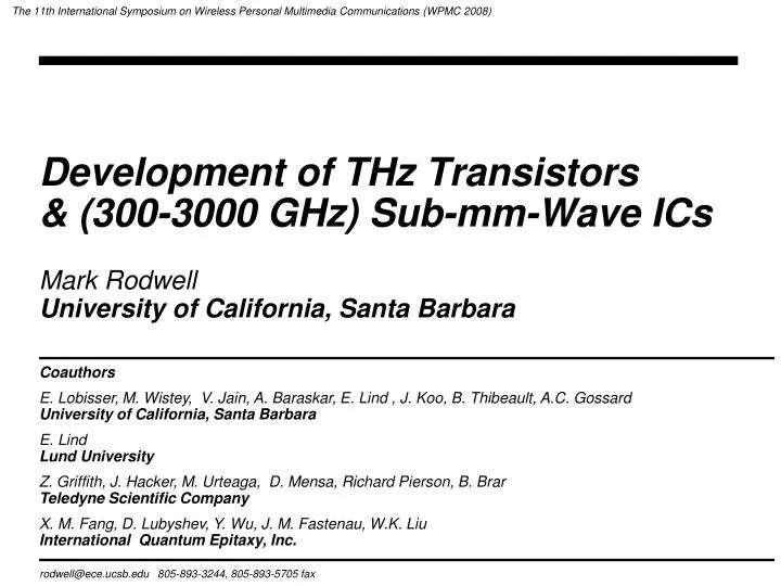
The 11th International Symposium on Wireless Personal Multimedia Communications (WPMC 2008). Development of THz Transistors & (300-3000 GHz) Sub-mm-Wave ICs. Mark Rodwell University of California, Santa Barbara. Coauthors

E N D
The 11th International Symposium on Wireless Personal Multimedia Communications (WPMC 2008) Development of THz Transistors& (300-3000 GHz) Sub-mm-Wave ICs Mark Rodwell University of California, Santa Barbara Coauthors E. Lobisser, M. Wistey, V. Jain, A. Baraskar, E. Lind , J. Koo, B. Thibeault, A.C. GossardUniversity of California, Santa Barbara E. LindLund University Z. Griffith, J. Hacker, M. Urteaga, D. Mensa, Richard Pierson, B. BrarTeledyne Scientific Company X. M. Fang, D. Lubyshev, Y. Wu, J. M. Fastenau, W.K. Liu International Quantum Epitaxy, Inc. rodwell@ece.ucsb.edu 805-893-3244, 805-893-5705 fax
UCSB High-Frequency Electronics Group THz InP Bipolar Transistors. III-V CMOS for Si VLSI InGaAs-channel MOSFETs for sub-22-nm scaling Ultra high frequency III-V ICs sub-mm-wave ICs 100-500 GHz digital logic 50-200 GHz Silicon ICs mm-waves: MIMO links, arrays, sensor networks fiber optics
Multi-THz Transistors Are Coming InP Bipolars: 250 nm generation: → 780 GHz fmax , 400 GHz ft , 5 V BVCEO 125 nm & 62 nm nodes→ ~THz devices IBM IEDM '06: 65 nm SOI CMOS → 450 GHz fmax , ~1 V operation Intel June '07: 45 nm / high-K / metal gateproduction 65 nm: ~250 GHz fmax → continued rapid progress What applications for III-V bipolars ? What applications for mm-wave CMOS ?
THz InP vs. near-THz CMOS: different opportunities InP HBT: THz bandwidths, good breakdown, analog precision & 340 GHz, 70 mW amplifiers (design)In future: 700 or 1000 GHz amplifiers ? J. Hacker (Teledyne) M. Jones(UCSB) 200 GHz digital logic (design)In future: 450 GHz clock rate ? → fast blocks for microwave mixed-signal Z. Griffith 25-40 GHz gain-bandwidth op-amps→ low IM3 @ 2 GHz In future: 200 GHz op-amps for low-IM3 10 GHz amplifiers? Z. Griffith M. Urteaga (Teledyne)
massive monolithic mm-wave arrays→ 1 Gb/s over ~1 km mm-wave imagingsensor networks mm-wave MIMO THz InP vs. near-THz CMOS: different opportunities 65 / 45 / 33 / 22 ... nm CMOS vast #s of very fast transistors ... having low breakdown, high output conductance what NEW mm-wave applications will this enable ? comprehensive equalization of ~100 Gb/s wireless, wireline, optical links
InP DHBTs: September 2008 250 nm 250 nm 600nm 350 nm
Bipolar Transistor Scaling Laws Changes required to double transistor bandwidth: Linewidths scale as the inverse square of bandwidth because thermal constraints dominate.
industry university→industry university2007-8 appearsfeasible maybe InP Bipolar Transistor Scaling Roadmap emitter 512 256 128 64 32 nm width16 8 4 2 1 m2 access r base 300 175 120 60 30 nm contact width, 20 10 5 2.5 1.25 m2 contact r collector 150 106 75 53 37.5 nm thick, 4.5 9 18 36 72 mA/m2 current density 4.9 4 3.3 2.75 2-2.5 V, breakdown ft 370 520 730 1000 1400 GHz fmax 490 850 1300 2000 2800 GHz power amplifiers 245 430 660 1000 1400 GHz digital 2:1 divider 150 240 330 480 660 GHz
512 nm InP DHBT 500 nm mesa HBT 150 GHz M/S latches 175 GHz amplifiers LaboratoryTechnology UCSB / Teledyne / GCS UCSB 500 nm sidewall HBT DDS IC: 4500 HBTs 20-40 GHz op-amps Production ( Teledyne ) Z. GriffithM. UrteagaP. RowellD. PiersonB. BrarV. Paidi Teledyne Teledyne / BAE Teledyne / UCSB 20 GHz clock f = 405 GHz fmax = 392 GHz Vbr, ceo = 4 V 53 dBm OIP3 @ 2 GHzwith 1 W dissipation
150 nm thick collector 200 GHz master-slavelatch design 256 nm GenerationInP DHBT 70 nm thick collector 4.7 dB Gain at 306 GHz. 340 GHz, 70 mW amplifier design 60 nm thick collector from one HBT Z. Griffith, E. Lind, J. Hacker, M. Jones
324 GHz Medium Power Amplifiers in 256 nm HBT ICs designed by Jon Hacker / Teledyne Teledyne 256 nm process flow- Hacker et al, 2008 IEEE MTT-S ~2 mW saturated output power
Can we make a 1 THz SiGe Bipolar Transistor ? emitter 18 nm width1.2 m2 access r base56 nm contact width, 1.4 m2 contact r collector15 nm thick 125 mA/m2 current density??? V, breakdown ft 1000 GHz fmax 2000 GHz PAs 1000 GHz digital 480 GHz(2:1 static divider metric) Simple physics clearly drives scaling transit times, Ccb/Ic → thinner layers, higher current density high power density → narrow junctions small junctions→ low resistance contacts Key challenge: Breakdown 15 nm collector → very low breakdown(also need better Ohmic contacts) Solutions Eliminating excess collector area would partly ease scaling Assumes collector junction 3:1 wider than emitter. Assumes contacts 2:1 wider than junctions
single-chip 300-600 GHz spectrometers(gas detection) sub-mm-wave communications 670-1000 GHz imaging systems What Would You Do With a THz Transistor ? High-Performance 2-20 GHz Microwave Systemshigh excess transistor bandwidth + precision design--> high linear, highly precise microwave systems microwave ADCs and DACsmore resolution & more bandwidth microwave op-amps high IP3 at low DC power translinear mixershigh IP3 at low DC power
linear response increasing feedback output power, dBm 2-tone intermodulation input power, dBm mm-wave Op-Amps for Linear Microwave Amplification DARPA / UCSB / Teledyne FLARE: Griffith & Urteaga Reduce distortion with strong negative feedback 300 GHz / 4 V InP HBT R. Eden measured 20-40 GHz bandwidth measured 54 dBm OIP3 @ 2 GHz new designs in fabrication simulated 56 dBm OIP3 @ 2 GHz
single-chip 300-600 GHz spectrometers(gas detection) sub-mm-wave communications 670-1000 GHz imaging systems What Would You Do With a THz Transistor ? High-Performance 2-20 GHz Microwave Systemshigh excess transistor bandwidth + precision design--> high linear, highly precise microwave systems microwave ADCs and DACsmore resolution & more bandwidth microwave op-amps high IP3 at low DC power translinear mixershigh IP3 at low DC power
150 & 250 GHz Bands for 100 Gb/s Radio ? Wiltse, 1997IEEE APS-Symposium, sealevel 4 km 9 km 125-150 GHz, 200-300 GHz: enough bandwidth for 100 Gb/s QPSK 150 GHz carrier, 100 Gbs/s QPSK radio: 30 cm antennas, 10 dBm power, fair weather→ 1 km range 150 GHz band: Expect ~10-20 dB/km attenuation for rainBut, for > 300 GHz : expect >30 db/km from 90% humidity
mm-wave (60-80 GHz) MIMO → wireless at 40+ Gb/s rates ? 70 GHz, 1 km, 16 elements, 2 polarizations, 3.6 x 3.6 meter array, 2.5 GBaud QPSK → 160 Gb/s digital radio ?
mm-Wave & Sub-mm-Wave Wireless Links The ICs will soon make this possibleSiGe BiCMOS: up to 150 GHz now, future uncertainSi CMOS: up to 150 GHz now, 200-300 GHz soon, low output powerInP HBT: up to 500 GHz now, up to 1000 GHz soon moderate to high power, moderate noise Propagation characteristics will determine applications Foul-Weather Attenuation, Highly Directional (LOS only) propagation Massive mm-wave IC complexity in future → aggressive system adaptations / corrections