Download
1 / 54
590 likes | 618 Views
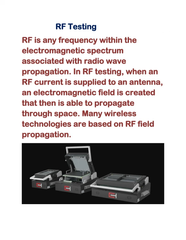
Fundamentals of RF Testing. Scalar vs Vector. There are many quantities that are measured independent of each other, and each is characterized by a single variable Resistance value, rms value of the sine wave, drain current of a transistor, etc.

E N D
Scalar vs Vector • There are many quantities that are measured independent of each other, and each is characterized by a single variable • Resistance value, rms value of the sine wave, drain current of a transistor, etc. • Other quantities have to be measured with multiple variables and only the combined value makes sensor. • The location of a flying object, the orientation of a satellite, the gain of a filter, the constellation of an OFDM signal, … • EVM: error vector measurement
When is a “wire” not a wire • For RF signals, wave length becomes very short • When a wire length is not much shorter than wave length, it cannot be considered a wire • Transmission line model must be used • If a wire length is not < 1/5 of wave length, antenna effect needs to be considered • If a wire length is not < 5% of wave length, voltages across wire are not the same
i R v Power of resistive device • P(t) = v(t)i(t)=v^2(t)/R=i^2(t)R >=0 for all t average power level P v i Amplitude Time
Z v Power in general devices • P(t) = v(t)i(t), could be positive, or negative P average power level i v Amplitude i Time
Average power • Integrate P(t) over one period of P(t) and divide by the period • If v(t) and i(t) are both periodic with the same frequency, P(t) is periodic with twice the frequency • Only need to integrate over half period of v(t) • If v and i have different frequency, P(t) will be periodic only if fv and fi are rationally related • Period of P is common period for v and I • Else, choose long enough of an interval T that is approximate integer multiples of Tv and Ti
Crest factor: CF = Ppeak/Pavg • For pulse signal: Pavg= Ppeak*DutyRatio = Ppulse*DutyRatio • RMS: Pavg=Vrms*Irms*cos(Df)
PPeak Peak power ofcombined wave 7 sinusoidal waves with 1V amplitude Power Pavg Time • Equation (12.25) is the worst case when all sinusoids match up in phase at the peak. • Normally the CF is much smaller • An earlier HW asked you to find phases to achieve small CF
70 60 50 40 30 20 10 0 0 50 100 150 200 250 300 PAPR in OFDM System • 52 Subcarriers: 17dB (=10*log52) PAPR
12000 10000 8000 6000 4000 2000 0 4 5 6 7 8 9 10 11 12 13 14 PAPR(dB) Peak Power Probability • Large peaks do not occur very often (Gaussian distribution)
HW • Write a Matlab program to generate a graph similar to what is given on the previous page.
Power transfer • Real power considered • Not complex power • For a given source • Power transferred to load depends on impedance matching • Max power transfer: • When ZL = Zs*, where * stands for complex conjugate • That is: RL = Rs, and XL = Xs simultaneously • Pmax = ½ |VA|2/Rs
Reflection Coefficient Rs jXs jXL Vs I V RL
Reflection Coefficient No reflectionMaximum power transfer
In general G is a complex number • For resistive network, you get a real number • For simplicity, you may want take the magnitude ratio to get a real number Use power ratio, instead,
Return Loss • Mismatch Loss
matched transmission line b) conjugate match a) matching network matching network matching network d Conjugate matching, by T, P networks
Power loss • Insertion loss, typically for filters • Filters used to suppress noise, distortions, interferences, etc. • But it cause power loss • IL = PL,1/PL,2
Transducer loss • A sensor or transduce generates a voltage (source) • If load is conjugate matched, it receive max power • This is the available power PA • With a given detection circuit, it may not be matched • Actual power to load is PL • Then TL = PA/PL
Noise • For an RF signal: v(t) = Aosin(wot + Qo) • Due to noise, both amplitude and phase may vary randomly with time v(t) = (Ao + a(t))sin(wot + Qo + f(t)) • These are called amplitude noise and phase noise • If there are no prio-knowledge, typically assume both components cause the same noise power
Noise figure and noise factor • For a circuit or system • Output SNR is always worse than input • Noise factor: F=SNRi/SNRo • Noise figure: NF = 10log10(F) • Noise figure always > 0, noise factor always > 1 system output input
Noise Factor As a function of device G: Power gain of the device
-40 -43dBm Output -60 -64dBm Power [dBm] -69dBm -80 Input -100 -120 2.4 2.5 2.45 Frequency [GHz] Find the noise figure -100dBm
2nd stage 1st stage Input Output B G2, Na2 B G1, Na1 Input Noise kT0B Na2 Na1 Total Noise added Total Noise Power output Na1G2 kT0BG1 kT0BG1G2 kT0B Cascaded system noise figureFsys=F1+(F2-1)/G1+(F3-1)/G2G1
Noise factor of Cascaded Stages Sin/Nin Sout/Nout G1, N1, F1 Gi, Ni, Fi GK, NK, FK • Overall NF dominated by F1 [1] F. Friis, “Noise Figure of Radio Receivers,” Proc. IRE, Vol. 32, pp.419-422, July 1944.
Warm up HW • Consider the following circuit. The passive filter is assumed noiseless. An RL is connected to the output but RL is assumed noiseless in the computation of the system noise figure. Compute the noise figure of the cascade connection.
HW Consider the following receiver chain. All filters are assumed to be noiseless. For each block, either power gain or voltage gain is marked. The amplifiers have matched input and output impedance and therefore their power gains are equal to their corresponding voltage gains in dB’s. The mixer’s power gain and voltage gain are different and are marked separately. The output is connected to a matched network but its noise contribution is already included in the noise figure of the amplifier. The noise introduced by the local oscillator is already included in the noise figure of the mixer. Compute the noise figure from nodes F, E, D, C, B, and A to G; compute the voltage gain from A to B, C, D, E, F, and G; and compute the power gain from A to B, C, D, E, F, and G.
Phase noise Amplitude Time PSD Frequency offset, Df a) Frequency, f b) Phase noise • v(t) = (Ao + a(t))sin(wot + Qo + f(t)) • Effects in time and frequency domain:
Typical measurement of phase noise • How many dB below carrier at a certain offset PS Power normalized to 1 Hz PSSB fc Frequency fc+Df
zs s21 TWO-PORT NETWORK a1 a2 s12 s22 s11 zL Vs b1 b2 S-parameters • Parameters for two-port system analysis • Suitable for distributive elements • Inputs and outputs expressed in powers • Transmission coefficients • Reflection coefficients I2 I1 zs s21 TWO-PORT NETWORK + + s12 s22 s11 zL V2 Vs V1 - - I2 I1
S-Parameters a1 b2 S21 S11 S22 S12 b1 a2
S-Parameters • S11 – input reflection coefficient with the output matched • S21 – forward transmission gain or loss • S12 – reverse transmission or isolation • S22 – output reflection coefficient with the input matched
S-Parameters I1 I2 S Z1 Z2 Vs1 V1 V2 Vs2
Stability Condition • Necessary condition where • Stable iff where
Losses • Given source impedance • Given load impedance • Given S-parameters Can compute: • Insertion Loss, IL • Return Loss, RL • Mismatch Loss, ML
Optional HW • Derive formulas for computing IL, RL, and ML.
HW Consider the simple circuit. • Calculate G=ioio*/VsVs* • Show that noise factor is • Compute the best F possible and determine how to achieve this. • From that, comment on power and process choices vs noise factor. • Compute S parameters. If necessary, make your assumptions on load. io Rs Vs Rs 4kTRs Vs Vgs gmVgs 4kTggm
Modulation • Important fact: a continuous, oscillating signal will propagate farther than other signals. • Start with a carrier signal • usually a sine wave that oscillates continuously. • Frequency of carrier fixed
Carrier Signal • In analog transmission, the sending device produces a high-frequency signal that acts as a basis for the information signal. • This base signal is called the carrier signal and its frequency is called carrier frequency • The receiving device is tuned to the frequency of the carrier that it expects from the sender.
Modulation • Digital information is modulated on the carrier signal by modifying one of its characteristics (amplitude, frequency, phase). • This modification is called modulation • Same idea as in radio, TV transmission • The information signal is called a modulating signal.
Modulation • Modulation: process of changing a carrier wave to encode information. • Modulation used with all types of media • Why is modulation needed? • Allows data to be sent at a frequency which is available • Allows a strong carrier signal to carry a weak data signal • Reduces effects of noise and interference
Types of modulation • Amplitude modulation (used in AM radio) – strength, or amplitude of carrier is modulated to encode data • Frequency modulation (used in FM radio) – frequency of carrier is modulated to encode data • Phase shift modulation (used for data) – changes in timing, or phase shifts encode data
Amplitude Modulation • Change amplitude in sync with information to be sent! Problems?
Frequency Modulation • Frequency of the carrier signal is modulated to follow the changing voltage level (amplitude) of the modulating signal. • Peak amplitude and phase of the carrier signal remain constant, but as the amplitude of the info signal changes, the frequency of the carrier changes accordingly.
Phase-Shift Modulation • vary phase of carrier • may use more than simply 180 degree shift (binary) • this allows higher bit rate than baud rate • Eight angles results in 3 bits per signal element. Or 3 bits per baud!
Output power: 16.2dBm 64QAM, 54Mb/s Average EVM: 3.41%, -29.3dB Transmit Constellation