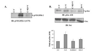
Download
1 / 36
360 likes | 519 Views
Russian Research Center Kurchatov Institute. Russian-Italian meeting December 11, 2009. Proposal on construction of new beamlines in spectral range 1 meV - 1.5 keV at the Kurchatov Center for SR and Nanotechnology. Kurchatov Center for Synchrotron Radiation and Nanotechnology.

E N D
Russian Research Center Kurchatov Institute Russian-Italian meeting December 11, 2009 Proposal on constructionof new beamlinesin spectral range 1 meV - 1.5 keV at the Kurchatov Center forSR andNanotechnology Kurchatov Center forSynchrotron Radiation andNanotechnology V. Stankevich
The analysis of world experience shows that more than 40% of experimental stations on synchrotron facilities are dedicated to investigations in the spectral range < 1.5 keV Synchrotron sources with electron beam energy 1.5-3 GeV
Fundamental characteristics of substances studied by up to 1.5 keV radiation We plan to add a wide range of experimental capabilities to the current facilities at the KCSR .
Siberia-2 storage ring: Ee = 2.5 GeV λc = 1.67 Å natural emittance = 76 nm*rad There are only 3 experimental stations using soft Siberia-1 storage ring radiation: - photoelectron spectroscopy FES station (20 - 100 eV); - optical investigation Lokus station (3 – 25 eV); - optical investigation Spectra station (3 – 200 eV) Siberia-1 storage ring: Ee = 450 MeV λc = 61 Å natural emittance = 880 nm*rad
PES IR id ML id PES id PES Optic ML
Beamline 3.1SPECTROLUMI SUPERLUMI, HASYLAB → SPECTROLUMI, Kurchatov Analysis of performance of SUPERLUMI • Presently, the demand for this type of measurements is higher than SUPERLUMI’s capacity. SUPERLUMI is expected to be closed as a part of DORIS III facility. • Advanced materials often require conventional types of investigation. The user community will benefit from access to a station of this type. • New type of information can be provided by luminescence spectroscopy with more extended excitation range than that provided by SUPERLUMI. • Combination of time-resolved luminescence spectroscopy with measurements of other secondary processes, such as photoemission, photoconductivity, desorption and induced absorption, would allow creating a full picture of energy relaxation processes in solids. We propose to create a new station in the Kurchatov Center of Synchrotron Radiation dedicated to the study of luminescence properties of various materials with the excitation range 5 eV to 1.5 keV. It will be the onlystation of this type in the world.
Layout Beamline 3.1SPECTROLUMI Siberia-2 undulator Optical scheme cooled focusing mirror NIM-PGM monochromator 5-1500 eV refocusing mirror slit refocusing mirror experimental chamber
Beamline 3.1SPECTROLUMI. Research areas Strong tradition of Russian luminescence research suggests the following directions of investigations performed at this station: Fluorescent materials and phosphors Scintillator materials Security Applications – ultra-high sensitivity required FEL Beam diagnostics Fluorescent lamps White LEDs High energy physics (LHC, Panda, …) – radiation hardness Geophysics – well monitoring Plasma displays Advanced Materials Medical applications – yield, time resolution, etc. Astrophysics and space research Meso- materials, superlattices, etc.
Beamline 4.1High-resolution UPSstation Super high-resolution UPS station requires undulator radiation with characteristic energy below 100 eV. The station is dedicated to high precision bandmapping of occupied electron states near Fermi level for single crystals in order to determine the dispersion relation of the electron energy versus the electron momentum (for example, measurements of superconducting gap for HTSC). Energy range: 10-320 eV Main experimental methods: super high energy and angle-resolved photoemission spectroscopy. Expected energy resolution: 3-5 meV.
Beamline 4.1High-resolution UPSstation cooled plane and focusing mirrors PGM monochromator 25-1500 eV slit experimental chamber, electron spectrometer refocusing mirror
Beamline 2.1SPELEEM (PES Microscope) Spectroscopic PhotoEmission and Low Energy Electron Microscopewith spatial resolution below 10 nm for nanotechnology research • Purpose of the microscope • The unit allows to obtain extremely useful information for resolving a wide range of nanotechnology problems: • investigations of pure single-crystal surfaces, • mapping of defects in complex chips, etc. • spatial or diffraction imaging of surfaces using secondary electrons with fixed kinetic energy. There are only 5 microscopes of this level in the world, and some are under construction at present time.
Electron analyzer MAX-Lab SPELEEM layout Projector Deflector Transfer Lens Photon beam Projector
Beamline 2.1SPELEEM (PES Microscope) Principal optical scheme Siberia-2 undulator cooled focusing mirror PGM monochromator 25-1500 eV undulator refocusing mirror slit SPELEEM refocusing mirror
Metrological Laboratoryat Kurchatov SR Source The project is aimed at the creation of a metrological complex based on several SR beamlines. The complex is dedicated to solving various photometry and radiometry problems. • Main applications: • diagnostics of SR source electron bunch and beam; • secondary sources calibration; • reflectometry; • detector calibrations; • metrological support EUV nanolithography (filters, mirrors, multilayers); • photobiological research (cytology, oncology); • standards development.
Metrological Laboratory Fourier IR spectrometer focusing mirror refocusing mirror entrance slit 3.5 m experimental chamber 2 m 7 m refocusing mirror 1-m normal monochromator (3-35 eV) Siberia-1
Metrological Laboratory Siberia-2 bending magnet cooled focusing mirror X-ray multilayer monochromator experimental X-ray hutch PGM monochromator refocusing mirror slit refocusing mirror experimental chamber
Advanced projects In addition to standard techniques there are some advanced proposals based on combination of different experimental methods.
Beamline 6.1: Universal Beamlinefor Infrared Spectroscopy and Spectromicroscopy • IR research features: • form oil inclusions in minerals to living tissues • image mapsof the charge carriers in nanometer-thick layer in organic FET • non-destructive and non-ionizing analysis methods; • red corpusclesin vivo Installation of 3 experimental stations will provide a number of techniques in a wide energy range 4 – 0.001 eV (30000 – 10 cm-1)
ALSBeamline 1.4.3:The voltage-induced IR absorption spectra of the organic FET (poly(3-hexylthiophene))- direct probe of the electronic excitations due to injected carriers: 1000–1500 cm-1 - polymer chain modes, 3500 cm-1 - polarons. Image map (right) – from scan beam spots 33 μm. The charge carriers are confined to a nanometer-thicklayer at the semiconductor–insulator interface, i.e. difficult to study using inelasticX-ray and neutron scattering, STM, photoemission spectroscopy. Использование ИК в нанотехнологии: органич. полевой транзистор
Beamline 6.1: Universal Beamlinefor Infrared Spectroscopy and Spectromicroscopy M2, M3 -refocusing toroidal mirrors top view Principal optical scheme experimental hutches D - diamond window 25 m M0 - cooled plane mirror M1- focusing elliptical mirror D 10 m Siberia-2 edge radiation
Beamline 6.1: Universal Beamlinefor Infrared Spectroscopy and Spectromicroscopy
IR combined with NEXAFS technique Conceptual layout of the beamline proposed by Laboratori Nazionali di Frascati.
Beamline 6.5:station “Surface” • Multipurpose station for: • bandmapping of occupied electron states near the Fermi level in single crystals in order to determine the dispersion relation for the electron energy versus the electron momentum; • low-dimensional and strongly correlated systems; • carbon, organic and bioorganic systems; • nanostructures, nanoclusters and nanodevice technology; • surface chemistry. Energy range: 25-1500 eV Experimental methods: • photoelectron spectroscopy PES • angle resolved PES (ARPES) • NEXAFS
Siberia-2 bending magnet Beamline 6.5station “Surface” Principal optical scheme cooled plane and focusing mirrors refocusing mirror PGM monochromator 25-1500 eV slit refocusing mirror experimental chamber, electron spectrometer, catalytic unit
KCSR NANOFACTORY – “NANOFAB 100” • NANOTECHNOLOGICAL FABRICATION FACILITY (NANOFAB-100) COMPRISES A CLUSTER OF WAFER–SIZE TECHNOLOGIES AND A CLUSTER OF NANO-LOCAL TECHNOLOGIES, INCLUDING: • PLASMA ETCHING • PULSED LASER DEPOSITION • FIB WITH DEPOSITION AND ION IMPLANTATION • UHV SCANNING PROBE MICROSCOPE • ATOMIC–FORCE MICROSCOPE WITH A LOCAL OF GAS INJECTION SYSTEM
KCSR NANOFACTORY – “NANOFAB 100” • NANOTECHNOLOGICAL FABRICATION FACILITY (NANOFAB-100), COMPRISING A CLUSTER OF WAFER–SIZE TECHNOLOGIES AND A CLUSTER OF NANO-LOCAL TECHNOLOGIES, INCLUDING: • PLASMA ETCHING • PULSED LASER DEPOSITION • FIB WITH DEPOSITION AND ION IMPLANTATION • UHV SCANNING PROBE MICROSCOPE • ATOMIC–FORCE MICROSCOPE WITH A LOCAL OF GAS INJECTION SYSTEM
Station “NanoSurface” • NANOTECHNOLOGICAL FABRICATION FACILITY (NANOFAB-100), COMPRISING A CLUSTER OF WAFER–SIZE TECHNOLOGIES AND A CLUSTER OF NANO-LOCAL TECHNOLOGIES, INCLUDING: • PLASMA ETCHING • PULSED LASER DEPOSITION • FIB WITH DEPOSITION AND ION IMPLANTATION • UHV SCANNING PROBE MICROSCOPE • ATOMIC–FORCE MICROSCOPE WITH A LOCAL OF GAS INJECTION SYSTEM combined with SR station “SURFACE”: • photoelectron spectroscopy PES • angle resolved PES (ARPES) • NEXAFS Unique capability: in situ step by step characterization of layered nanostructures and nanosystems
Station “NanoSurface” NANOFAB-100 station SURFACE beamline Class ISO 6 clean room Siberia-2 bending magnet
Station “NanoSurface” NANOFAB compatible modules revolver type sample storage and distribution module station “SURFACE”:experimental chamber monochromatized SR
TECHNOLOGIES OF MOLECULAR SELF–ASSEMBLY. MATERIALS POSSESSING “NATURAL” PROPERTIES, E.G. SELF–CLEANING AND NON–WETTING SURFACES ANISOTROPIC AND BIOMIMETIC MATERIALS GRAPHENE AND SYSTEMS ON ITS BASIS. SURFACES WITH HIGH ABSORPTION OF OPTICAL AND ELECTROMAGNETIC RADIATION INNOVATIVE ELECTRONIC MATERIALS TECHNOLOGIES OF MATERIALS AND NANOSTRUCTURES CAPABLE OF ADAPTING THEIR PROPERTIES UNDER THE INFLUENCE OF EXTERNAL FACTORS. ADAPTIVE NANO– AND META MATERIALS MATERIALS AND STRUCTURES CAPABLE OF CONVERTING AMBIENT NATURAL ENERGY (SOLAR, HEAT AND CHEMICAL GRADIENTS, ETC.) INTO ELECTRICITY. CLEANTECH: ENERGY HARVESTING MATERIALS RESEARCH PLANS AND EXPECTED RESULTS
Thank you for your attention!We are looking forward to a fruitful collaboration.