Download
1 / 33
330 likes | 338 Views
Electronics Transistors. Dr. Walid Mohiyeldin Ibrahim IT Department. Transistor Characteristic & Parameters. Transistor Operating Regions: 1.Cutoff region: Both transistor junctions are reverse biased All terminal current are approximately equal to zero 2.Active region :

E N D
Electronics Transistors Dr. Walid Mohiyeldin Ibrahim IT Department
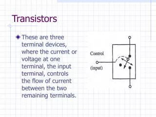
Transistor Characteristic & Parameters Transistor Operating Regions: 1.Cutoff region: • Both transistor junctions are reverse biased • All terminal current are approximately equal to zero • 2.Active region: • The BE junction is forward biased and the BC junction is reverse biased • All terminal currents have some measurable value • The magnitude of IC depends on the values of and IB • VBE is approximately 0.7V and VCE falls in ranges VBE<VCE<VCC • 3.Saturation: • Both transistor junctions are forward biased • IC reaches its maximum values- determine by the component in the CE circuit, and independent of the values of and IB • VBE must be greater than a threshold voltage. • VB must be higher than both VE and VC. Also VBC < VBE and VBE > 0 leakage current is neglected
Transistor Characteristic & Parameters (cont.) More About beta, : -Important parameter for BJT -Varies both IC & temperature -Keeping the junction temperature constant, IC cause -Further increase in IC beyond this max. point cause to decrease Maximum Transistor Ratings: -Specified on manufacturer’s data sheet -Given for VCE,VBE,VBC,IC & power dissipation -The product of VCE and IC must not exceed the max. power dissipation -Both VCE and IC cannot be max. at the same time.
Transistor Characteristic & Parameters (cont.) Current and Voltage Analysis: • The base current is: • The dc voltage at the collector w.r.t the emitter: where IE = IC + IB • IC ≈ IE • The voltage at the collector w.r.t the base:
Transistor Characteristic & Parameters (cont.) Current and Voltage Analysis: • The voltage at the collector with respect to the grounded emitter is • Since the drop across is: • The dc voltage at the collector w.r.t the emitter: where • The voltage at the collector w.r.t the base: (5) (6)
Example • Determine the following for the fixed-bias configuration • (a) IBand IC. • (b) VCE. • (c) VBand VC. • (d) VBC.
Transistor Saturation • The term saturation is applied to any system where levels have reached their max values. • In the saturation conditions the base–collector junction is no longer reverse-biased and the output amplified signal will be distorted.
Relation of β • Repeat the calculation for β =100 • The BJT collector current is seen to change by 100% due to the 100% change in the value of β. • IBis the same • VCEdecreased by 76%.
Emitter-stabilized Bias Circuit • Emitter-stabilized circuit includes a resistor at the emitter terminal • This emitter resistor provides improved temperature stability over fixed bias configuration
Base-Emitter Loop • From Kirchhoff’s voltage law • Recall that • Substituting for IE • Solving for IB gives
Collector–Emitter Loop • From Kirchhoff’s voltage law • Substituting IE ≈ IC and grouping terms gives • The voltage at the collector can be determined • The voltage at the base can be determined
Example • Find IB, IC, VCE, VC, VE, VB and VBC
Relation with β • Repeat the calculation for β =100 • Now the BJT collector current increases by about 81% due to the 100% increase in β. • Notice that IBdecreased, helping maintain the value of IC. • The change in VCEhas dropped to about 35%.
VOLTAGE-DIVIDER BIAS • In the previous bias configurations the bias current ICand voltage VCEwere a function of the current gain (β) of the transistor. • However, since β is temperature sensitive, especially for silicon transistors, and the actual value of beta is usually not well defined, it would be desirable to develop a bias circuit that is less dependent.
VOLTAGE-DIVIDER BIAS • If the circuit parameters are properly chosen, the resulting levels of IC and VCEcan be almost totally independent of beta. • There are two methods that can be applied to analyze the voltage divider. • The exact method that can be applied to any voltage-divider configuration. • The approximate method and can be applied only if specific conditions are satisfied.
VOLTAGE-DIVIDER BIAS – Exact Analysis • RTh: Replace the 2 parallel resistance as follow:
VOLTAGE-DIVIDER BIAS – Exact Analysis • ETh: represent the voltage source Vcc, R1 and R2 using voltage divider rule as follow: VCC – VR1 - VR2 = 0 VCC – IR1 - IR2 = 0 Since VR2 = IR2
VOLTAGE-DIVIDER BIAS – Exact Analysis • The Thévenin network is then redrawn as shown • IBcan be determined by first applying Kirchhoff’s voltage law ETh - IBRTh - VBE -IERE = 0 • Substituting IE = (β + 1)IBand solving for IByields
VOLTAGE-DIVIDER BIAS – Exact Analysis • Once IBis known, the remaining quantities of the network can be found in the same manner
Example • Find IB, IC, VCE, VC, VE, VB and VBC
VOLTAGE-DIVIDER BIAS – Approximate Analysis • The input section of the voltage-divider configuration can be represented as follow. • The resistance Ri is the equivalent resistance between base and • ground for the transistor with an emitter resistor RE. • If Riis much larger than the resistance R2 the current IB will be much smaller than I2 • (current always seeks the path of least resistance) • I2 will be approximately equal to I1. • The voltage across R2, which is actually the base voltage, can be determined using the voltage-divider rule
VOLTAGE-DIVIDER BIAS – Approximate Analysis VCC – VR1 - VR2 = 0 VCC – IR1 - IR2 = 0 Since VR2 = IR2 • Since Ri = ( β + 1)RE ≈ βREthe condition that will define whether the approximate approach can be applied will be the following:
VOLTAGE-DIVIDER BIAS – Approximate Analysis • Once VBis determined, the level of VEcan be calculated from • The emitter current can be determined from • The collector-to-emitter voltage is determined by • Note in this sequence of calculations that β does not appear and IBwas not calculated. • The Q-point (as determined by ICQ and VCEQ) is therefore independent of the value of .
Example • Repeat the previous analysis using the approximate technique, and compare solutions for ICand VCE.