Download
1 / 37
390 likes | 585 Views
Transistors. They are unidirectional current carrying devices with capability to control the current flowing through them The switch current can be controlled by either current or voltage Bipolar Junction Transistors ( BJT ) control current by current

E N D
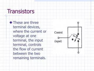
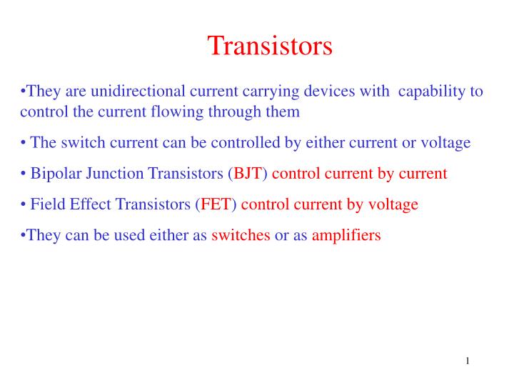
Transistors • They are unidirectional current carrying devices with capability to control the current flowing through them • The switch current can be controlled by either current or voltage • Bipolar Junction Transistors (BJT) control current by current • Field Effect Transistors (FET) control current by voltage • They can be used either as switches or as amplifiers
NPN Bipolar Junction Transistor • One N-P (Base Collector) diode one P-N (Base Emitter) diode
PNP Bipolar Junction Transistor • One P-N (Base Collector) diode one N-P (Base Emitter) diode
BJT and • From the previous figureiE = iB + iC • Define = iC / iE • Define = iC / iB • Then = iC / (iE –iC) = /(1- ) • TheniC = iE; iB = (1-) iE • Typically 100 for small signal BJTs (BJTs that • handle low power) operating in active region (region • where BJTs work as amplifiers)
BJT in Active Region Common Emitter(CE) Connection • Called CE because emitter is common to both VBB and VCC
BJT in Active Region (2) • Base Emitter junction is forward biased • Base Collector junction is reverse biased • For a particular iB, iCis independent of RCC • transistor is acting as current controlled current source (iC is controlled by iB, and iC= iB) • Since the base emitter junction is forward biased, from Shockley • equation
Early Effect and Early Voltage • As reverse-bias across collector-base junction increases, width of the collector-base depletion layer increases and width of the base decreases (base-width modulation). • In a practical BJT, output characteristics have a positive slope in forward-active region; collector current is not independent of vCE. • Early effect: When output characteristics are extrapolated back to point of zero iC, curves intersect (approximately) at a common point vCE = -VA which lies between 15 V and 150 V. (VA is named the Early voltage) • Simplified equations (including Early effect): Chap 5 - 8
BJT in Active Region (3) • Normally the above equation is never used to calculateiC, iB • Since for all small signal transistors vBE 0.7. It is only useful for deriving the small signal characteristics of the BJT. • For example, for the CE connection, iB can be simply calculated as, or by drawing load line on the base –emitter side
iB 100 A 0 5V vBE Deriving BJT Operating points in Active Region –An Example In the CE Transistor circuit shown earlier VBB= 5V, RBB= 107.5 k, RCC = 1 k, VCC = 10V. Find IB,IC,VCE,and the transistor power dissipation using the characteristics as shown below By Applying KVL to the base emitter circuit By using this equation along with the iB / vBE characteristics of the base emitter junction, IB = 40 A
iC 100 A 10 mA 80 A 60 A 40 A 20 A 0 20V vCE Deriving BJT Operating points in Active Region –An Example (2) By Applying KVL to the collector emitter circuit By using this equation along with the iC / vCE characteristics of the base collector junction,iC = 4 mA, VCE = 6V Transistor power dissipation = VCEIC = 24 mW We can also solve the problem without using the characteristics if and VBE values are known
BJT in Cutoff Region • Under this condition iB= 0 • As a result iC becomes negligibly small • Both base-emitter as well base-collector junctions may be reverse • biased • Under this condition the BJT can be treated as an off switch
BJT in Saturation Region • Under this condition iC / iB in active region • Both base emitter as well as base collector junctions are forward • biased • VCE 0.2 V • Under this condition the BJT can be treated as an on switch
BJT in Saturation Region (2) • A BJT can enter saturation in the following ways (refer to the CE circuit) • For a particular value ofiB,if we keep on increasing RCC • For a particular value ofRCC,if we keep on increasing iB • For a particular value ofiB,if we replace the transistor with one with higher
iC 100 A 10 mA 80 A 60 A 40 A 20 A 0 20V vCE BJT in Saturation Region – Example 1 In the CE Transistor circuit shown earlier VBB= 5V, RBB= 107.5 k, RCC = 10 k, VCC = 10V. Find IB,IC,VCE,and the transistor power dissipation using the characteristics as shown below Here even though IB is still 40 A; from the output characteristics, IC can be found to be only about 1mA and VCE 0.2V( VBC 0.5V or base collector junction is forward biased (how?)) = IC / IB = 1mA/40 A = 25 100
BJT in Saturation Region – Example 2 In the CE Transistor circuit shown earlier VBB= 5V, RBB= 43 k, RCC = 1 k, VCC = 10V. Find IB,IC,VCE,and the transistor power dissipation using the characteristics as shown below Here IB is 100 A from the input characteristics; IC can be found to be only about 9.5 mA from the output characteristics and VCE 0.5V( VBC 0.2V or base collector junction is forward biased (how?)) = IC / IB = 9.5 mA/100 A = 95 100 Transistor power dissipation = VCEIC 4.7 mW Note: In this case the BJT is not in very hard saturation
iC iB 100 A 100 A 80 A 60 A 40 A 20 A 0 0 20V vCE 5V vBE Output Characteristics BJT in Saturation Region – Example 2 (2) 10 mA Input Characteristics
BJT in Saturation Region – Example 3 In the CE Transistor circuit shown earlier VBB= 5V, VBE = 0.7V RBB= 107.5 k, RCC = 1 k, VCC = 10V, = 400. Find IB,IC,VCE, and the transistor power dissipation using the characteristics as shown below By Applying KVL to the base emitter circuit Then IC= IB= 400*40 A = 16000 A and VCE = VCC-RCC* IC =10- 0.016*1000 = -6V(?) But VCE cannot become negative (since current can flow only from collector to emitter). Hence the transistor is in saturation
BJT in Saturation Region – Example 3(2) Hence VCE 0.2V IC = (10 –0.2) /1 = 9.8 mA Hence the operating = 9.8 mA / 40 A = 245
BJT ‘Q’ Point (Bias Point) • Q point means Quiescent or Operating point • Very important for amplifiers because wrong ‘Q’ point selection increases amplifier distortion • Need to have a stable ‘Q’ point, meaning the the operating point should not be sensitive to variation to temperature or BJT, which can vary widely
Four Resistor bias Circuit for Stable ‘Q’ Point By far best circuit for providing stable bias point
Analysis of 4 Resistor Bias Circuit (2) Applying KVL to the base-emitter circuit of the Thevenized Equivalent form VB - IB RB -VBE - IE RE = 0(1) Since IE = IB + IC = IB + IB= (1+ )IB (2) Replacing IE by (1+ )IB in (1), we get (3) If we design(1+ )RE RB (say (1+ )RE 100RB) Then (4)
Analysis of 4 Resistor Bias Circuit (3) And (for large ) (5) Hence IC and IE become independent of ! Thus we can setup a Q-point independentof which tends to vary widely even within transistors of identical part number (For example, of 2N2222A, a NPN BJT can vary between 75 and 325 for IC = 1 mA and VCE = 10V)
4 Resistor Bias Circuit -Example A 2N2222A is connected as shown with R1 = 6.8 k,R2 = 1 k,RC = 3.3 k, RE = 1 k and VCC = 30V. Assume VBE = 0.7V. Compute VCC and IC for = i)100 and ii) 300
4 Resistor Bias Circuit –Example (1) i) = 100 ICQ = IB = 3.09 mA IEQ = (1+)IB = 3.12 mA VCEQ = VCC-ICRC-IERE = 30-3.09*3.3-3.12*1=16.68V
4 Resistor Bias Circuit –Example (2) i) = 300 ICQ = 300IB = 3.13 mA IEQ = (1+)IB = 3.14 mA VCEQ = VCC-ICRC-IERE = 30-3.13*3.3-3.14*1=16.53V
= 300 ICQ = 100 VCEQ 16.68 V 16.53 V 0.9 % 3.09 mA 3.13 mA 1.29 % % Change 4 Resistor Bias Circuit –Example (3) The above table shows that even with wide variation of the bias points are very stable.
Four-Resistor Bias Network for BJT F. A. region correct - Q-point is (201 mA, 4.32 V)
Four-Resistor Bias Network for BJT (cont.) • All calculated currents > 0, VBC = VBE - VCE = 0.7 - 4.32 = - 3.62 V • Hence, base-collector junction is reverse-biased, and assumption of forward-active region operation is correct. • Load-line for the circuit is: The two points needed to plot the load line are (0, 12 V) and (314 mA, 0). Resulting load line is plotted on common-emitter output characteristics. IB = 2.7 mA, intersection of corresponding characteristic with load line gives Q-point.
Four-Resistor Bias Network for BJT: Design Objectives • We know that • This implies that IB << I2, so that I1 = I2. So base current doesn’t disturb voltage divider action. Thus, Q-point is independent of base current as well as current gain. • Also, VEQ is designed to be large enough that small variations in the assumed value of VBE won’t affect IE. • Current in base voltage divider network is limited by choosing I2 ≤ IC/5. This ensures that power dissipation in bias resistors is < 17 % of total quiescent power consumed by circuit and I2 >> IB for b > 50.
Four-Resistor Bias Network for BJT: Design Guidelines • Choose Thévenin equivalent base voltage • Select R1 to set I1 = 9IB. • Select R2 to set I2 = 10IB. • RE is determined by VEQ and desired IC. • RC is determined by desired VCE.
Four-Resistor Bias Network for BJT: Example • Problem: Design 4-resistor bias circuit with given parameters. • Given data: IC = 750 mA,bF = 100, VCC = 15 V, VCE = 5 V • Assumptions: Forward-active operation region, VBE = 0.7 V • Analysis: Divide (VCC - VCE) equally betweenREandRC. Thus, VE = 5 V • and VC = 10 V
Two-Resistor Bias Network for BJT: Example • Problem: Find Q-point for pnp transistor in 2-resistor bias circuit with • given parameters. • Given data: bF = 50, VCC = 9 V • Assumptions: Forward-active operation region, VEB = 0.7 V • Analysis: Forward-active region operation is correct Q-point is : (6.01 mA, 2.88 V)