Download
1 / 32
390 likes | 840 Views
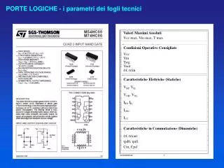
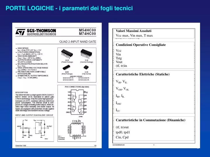
PORTE LOGICHE - i parametri dei fogli tecnici. Valori Massimi Assoluti Vcc max, Vin max, T max. Condizioni Operative Consigliate Vcc Vin Tstg Vout (tf, tr)in. Caratteristiche Elettriche (Statiche) V IH , V IL V OH , V OL I IH , I IL I OSC I CC.

E N D
PORTE LOGICHE - i parametri dei fogli tecnici Valori Massimi Assoluti Vcc max, Vin max, T max Condizioni Operative Consigliate VccVinTstgVout(tf, tr)in Caratteristiche Elettriche (Statiche) VIH, VIL VOH, VOL IIH, IIL IOSC ICC Caratteristiche in Commutazione (Dinamiche) (tf, tr)outtpd0, tpd1Cin, Cpd
Vin Vcc t tpd Vout Vcc t tf PORTE LOGICHE - le anomalie Vin Vout molteplici anomalie: - livelli logici NON ideali - ritardo di commutazione - segnali trapezoidali - derive termiche, ecc
A B 5V 5V 2,4V Transfer caratheristic 2,0V 5 4 3 2 1 0 0,8V 0,4V 0 0 in B out A Output voltage (V) famiglia VIH VIL VOH VOL TTL 2,0 V 0,8 V 2,4 V 0,4 V LS-TTL 2,0 V 0,8 V 2,7 V 0,5 V 0 1 2 3 4 5 Input voltage (V) param. conditions min typ max units VOH Vcc=4.5V, 70°C, Io= -0.4mA, Vin=0.8V 2.4 3.3 V VOL Vcc=4.5V, 70°C, Io=16mA, Vin=2V 0.22 0.4 V PORTE LOGICHE - i livelli logici incertezza
schema internodi una porta TTL(Nand a 2 ingressi) circuito equivalente d’ingresso Vcc Vcc IIH 4K param min max units IIH 40 µA RIN 100 Kohm IIL -1.6 mA InA Vout Vcc Gnd IIL Gnd InB PORTE LOGICHE - le correnti d’ingresso
schema internodi una porta TTL(Nand a 2 ingressi) circuito combinatore e traslatore Vcc 100 RL param min max units IOH -13 mA IOL 25 mA IOSC -55 mA circuito combin. e trasl. VOL Out IOL PORTE LOGICHE - le correnti d’uscita
circuito combinatore e traslatore Vcc 100 param min max units IOH -13 mA IOL 25 mA IOSC -55 mA IOH Out RL PORTE LOGICHE - le correnti d’uscita schema internodi una porta TTL(Nand a 2 ingressi) circuito combin. e trasl. VOH
Vin tpd = Propagation Delay Time(tempo di propagazione) è il ritardo con cui l’uscita della logica commutarispetto all’istante in cui commuta l’ingresso t tpd Vout A OUT B t VA param. typ max units tpd0 8 12 nsec tpd1 12 18 nsec VB tpd Vout PORTE LOGICHE - il tempo di propagazione
PORTE LOGICHE - i tempi di salita e discesa V1 t Vout V2 t t tf tr
Vcc Vcc 100 4K Out IIL IOL Gnd PORTE LOGICHE - il fan-out n° porte RIN IIL 1 4K -1.6mA2 2K -3.2mA5 0.8K -8mA10 0.4K -16mA15 0.27K -24mA Il FAN-OUT rappresenta il massimo numero di porte logiche pilotabili da un’uscita, ed è equivalente al rapporto frala massima corrente d’uscita e la massima corrente d’ingresso
NOR o NAND ? PORTE LOGICHE - RTL e DTL
PORTE LOGICHE - il circuito delle TTL
2.1V 1.4V 0.7V PORTE LOGICHE - il circuito delle TTL: ingressi aperti 0.9V 0.9V 0.2V
SAT PORTE LOGICHE - il circuito delle TTL: un ingresso a massa SAT 4.3V se Io = 0 0.2V INT INT
5V 4 3 2 1 0 0 5 10 15 20 mA PORTE LOGICHE - la tensione d’uscita è funzione della corrente Vo = Vcc - R·Io - VCE(SAT) - 0.7
LOGICHE STANDARD LOGICHE TTL (bipolari) LOGICHE CMOS 7400 TTL 4011 Cmos PORTE LOGICHE - varie famiglie - 7400 TTL- 74S00 Schottky-TTL- 74LS00 Low-Power S-TTL- 74AS00 Advanced S-TTL- 74ALS00 Advanced LS-TTL - 4000 CMOS classiche - 74HC00 High-Speed Cmos pin-compatibile TTL - 74HCT00 High-Speed Cmos pin-compatibile TTL level-compatible TTL
parametro 74xx 74LS 4000 74HCT unità Vcc nominale 5±10% 5±5% 3...15 2…6 V Vcc massima 8 5.5 20 7 V Pd/gate typ- 10 8 10-3 10-2 mW Fan Out 10 10 50 10 - - tpd typ 10 5 60 8 nsec freq. massima 20 40 5 30 MHz VIH (minima) 2 2 3.5 2 V VIL (massima) 0.8 0.8 1.5 0.8 V VOH (minima) 2.4 2.7 4.95 4.9 V VOL (massima) 0.4 0.5 0.05 0.1 V IIH massima 0.1 0.1 10-6 10-4 mA IIL massima -1.6 -0.4 -10-6 -10-4 mA IOSC massima -55 -100 -2 -40 mA PORTE LOGICHE - un confronto
velocità (tpd) tempi di salita/discesa (tf, tr) dissipazione (Pd/gate) fan-out tensione di alimentazione integrabilità Parametri-chiave: PORTE LOGICHE - l’evoluzione 1960:logiche RTL (Resistor-Transistor Logic) 1965:logiche DTL (Diode-Transistor Logic) 1970:logiche TTL (Transistor-Transistor Logic) 1972:logiche HLL (High-Level Logic) 1975:logiche CMOS (Complementary Metal-Oxyde Semiconductor) 1980:logiche Schottky (S-TTL, AS, LS, FAST) 1990:logiche HCmos (High-Speed Cmos Logic) 1995:logiche BiCmos (Bipolar & Cmos Logic)