Download
1 / 17
170 likes | 177 Views
ETD PID meeting. We had 5 presentations dedicated to electronics Fe barrel electronics status Backplane and PM positioning Study of the Hamamatsu @ Milano lab Study of the Hamamatsu 8500 @ Bari New developments on the electronics for the FTOF. On behalf of PID group.

E N D
ETD PID meeting • We had 5 presentations dedicated to electronics • Fe barrel electronics status • Backplane and PM positioning • Study of the Hamamatsu @ Milano lab • Study of the Hamamatsu 8500 @ Bari • New developments on the electronics for the FTOF • On behalf of PID group Christophe Beigbeder/ ETD PID meeting
H8500 studies w/o amplification : Charge Map Photocathode Focusing electrode Dynode 1 Dynode 2 Dynode 3 We have found, as expected, that the there is an effect in gain that seems to increase a little bit (+5%) near the focusing electrode
H8500 studies w/o amplification : Jitter Map We have also found that there is an effect on timing performance of the device. Near the focusing electrode the jitter increase of almost 100ps and the transit time is 250ps shorter
In view of the LHCb upgrade, a possible option is to substituting the HPD with commercial multi-anode photomultiplier tube. The Milano-Bicocca group has worked on this, characterizing first the Hamamatsu H9500, then the R7600 and now R11265 for fast single photon response. Comparison between single photon spectra and dark events Gain reduction effect due to aging R11265: Single photon peak and dark events gain reduced to about 50% after 1600h hours. R11265: Gain vs Bias Voltage Only 120 crosstalk signals are above the threshold chosen for the main signal. ↓ 120 / 50000 = 0.24% At -850V the mean signal is about 1.9 Mel1.9 Mel
R7600: Voltage distribution ratio and single photon peak R7600: Gain reduction effect due to the magnetic field Changing the bias voltage ratio allows to sharpen the peak in the single photon spectra. R7600: TTS evaluation different pairs of pixel were measured: In all cases, the standard deviation of the time difference was about 300 ps. H9500 & R7600 has some drawbacks and the more attractive seems to be the R11265 -> test with the CLARO chip@ Cern in 2012 s = 301 ps
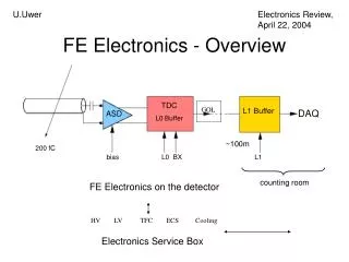
Electronics on the detector • We are working on the integration of the electronics on the detector: mechanical and electronics issues to connect the FE boards to the PM on the detector. Christophe Beigbeder
Backplane PM We had discussions on the way we are inserting boards with respect to the alignment of the PM, the tolerance on the connector position on the backplane Christophe Beigbeder
Electronics Chain : 16 Channel processing block diagram FPGA ProsAsic 3 PM pulse • ~ 50 Gb/s. Data pushed • L1 derandomizer here ! Max 100 KHz/ch TDC part Readout part Christophe Beigbeder
The front end crate Front end crate: PM Backplane – Communication backplane – FE board - FBLOCK controller (FBC Christophe Beigbeder
SCATS test board General synoptic • 10 TDC SCATS has been delivered in February, one month earlier than expected ! 5 are for each of the two labs, LAL and LPC Caen. • Test board expected mid April. Gaussian distribution pattern stored in RAM
Analog board : first result Analog board test 3 different solutions for low walk discriminator. Two analog boards was delivered last month @ LPNHE Input signal ~ 8mv pp average Dynamic ~10- Noise to be studied Discri output Gain , CFD fraction & delay , pseudo CFD integration has to be tuned Christophe Beigbeder
PIF : a design test for SCATS Analog pipeline : could be skipped in the first version for time and cost reasons Pseudo CFD , and charge amplifier For cost reasons, we will design the “ analog “ part of the TDC SCATS , in a dedicated chip : PIF. PIF will be submitted end of this year.
Parametric simulation : amplitude from 1 to 10 45ps walk • Resolution: • 50ps for a dynamic of 10
Possibility to add an individual DC offset on each signal • Possibility to chain channels by groups of 2 • 2 individual trigger discriminators on each channel • External and internal trigger + numerous modes of triggering on coïncidence (11 possibilities including two pulses on the same channel => useful for afterpulse studies • Embedded digital CFD for time measurement • Embedded signal amplitude extraction • Embedded charge mode (integration starts on threshold or at a fixed location) => high rates (~ 3.5 kEvents/s) • 2 extra memory channels for digital signals • One pulse generator on each input • External clock input for multi-board applications • Embedded USB and Serial Lite/Fibre Channel/Conet interfaces • Possibility to program the FPGAs via USB/Backplane/Altera Blaster • This board house the SAMLONG (1024 cells/ch) ASICs • The boardcanbeconnected to a backplane • possibility to scale the system up to 320 channels • in a crate
Preliminary results • We send pulses from a pulse generator (1V pp, rise & fall time: 1.6 ns, FWHM 2 ns) • We vary the distance. Time jitter between two channels THE SAME SAMLONG chip DIFFERENT SAMLONG chip: Δt ~ 0 ns (Ch1 – Ch0) jitter = 4.2 ps rms Δt ~ 10 ns (Ch1 – Ch0) jitter = 7.0 ps rms Δt ~ 0 ns (Ch1 – Ch0) jitter = 8.3 ps rms Δt ~ 10 ns (Ch1 – Ch0) jitter = 9.6 ps rms
SAMPIC: the ps TDC for FTOF Critical path for time measurement • Westarteddesigning the SAMPIC ps TDC a few monthsago => This ASIC makes use of the new AMS 0.18 µm CMOS technology • First version will house 8 blocks of 64 analog memory cells • Samplingisperformedbetween 2 and 10 GS/s • Signal bandwidthis ~ 1 GHz • Digitizationwillbeperformedinside the chip with a parallel Wilkinson ADC running at 2 GHz in eachcell • The 2-GHz clockis not distributed to the cells but runs a unique gray counter • The cells house a fastcomparator and a latch • Submissionistargetted for nextmonth-> First tests shouldtake place in July
Next step @ schedule • Test of the analog board using the PM test setup at LAL (Orsay) and Bari • Characterization of PM continue • Firmware and software are developed in Orsay and Bari to prepare the SCATS test, link to the CRT acquisition system. • Simulation and design of the PIF continue. • Work on backplane and integration continue • PIF submission end of 2012. SAMPIC next month. • TDR to be completed Christophe Beigbeder