Download
1 / 2
20 likes | 27 Views
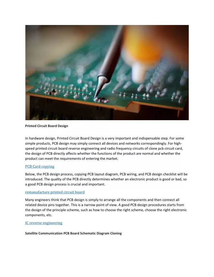
In hardware design, Printed Circuit Board Design is a very important and indispensable step. For some simple products, PCB design may simply connect all devices and networks correspondingly. For high-speed printed circuit board reverse engineering and radio frequency circuits of clone pcb circuit card, the design of PCB directly affects whether the functions of the product are normal and whether the product can meet the requirements of entering the market.

E N D
Printed Circuit Board Design In hardware design, Printed Circuit Board Design is a very important and indispensable step. For some simple products, PCB design may simply connect all devices and networks correspondingly. For high- speed printed circuit board reverse engineering and radio frequency circuits of clone pcb circuit card, the design of PCB directly affects whether the functions of the product are normal and whether the product can meet the requirements of entering the market. PCB Card copying Below, the PCB design process, copying PCB layout diagram, PCB wiring, and PCB design checklist will be introduced. The quality of the PCB directly determines whether an electronic product is good or bad, so a good PCB design process is crucial and important. remanufacture printed circuit board Many engineers think that PCB design is simply to arrange all the components and then connect all related device pins together. This is a narrow point of view. A good PCB design procedures starts from the design of the principle scheme, such as how to choose the right scheme, choose the right electronic components, etc. IC reverse engineering Satellite Communication PCB Board Schematic Diagram Cloning
Successful Satellite Communication PCB Board Schematic Diagram Cloning requires careful attention to every step and every detail throughout the PCB board reverse engineering process, which means thorough and careful planning at the beginning of the high frequency printed circuit board design cloning phase, and a comprehensive and continuous evaluation of the progress of each design step. redesign PCB circuit board Satellite Communication PCB Board Schematic Diagram Cloning requires careful attention to every step and every detail throughout the PCB board reverse engineering process And this kind of meticulous design skills is what most electronic enterprise cultures lacked. In recent years, due to the demand and growth of Bluetooth devices, wireless local area network (WLAN) devices, and mobile phones, the industry has paid more and more attention to the skills of RF circuit schematic diagram cloning. reverse engineering PCB From the past until now, radio frequency circuit board design cloning has always been the most difficult part for engineers to control, even a nightmare, just like electromagnetic interference (EMI) problems. Satellite Communication PCB Board Schematic Diagram Cloning right the first time requires careful planning and attention to detail to be effective. Radio frequency (RF) circuit board design is often described as a “black art” because there are still many uncertainties in theory. But this is only a partial view, and there are still many rules that can be followed in RF circuit board design. In actual design, however, the real trick is how to trade off these laws when they cannot be implemented due to various constraints. Important RF design topics include: Impedance and Impedance Matching, Insulator Materials and Laminates, Wavelength and Harmonics…etc. In the development process of WiFi products, the wiring of radio frequency circuits (RF Circuit Layout Guide) is a very critical process. In many cases, we may have a perfect design in principle, but in the actual board manufacturing, it is found that it is not ideal after the upper part. In fact, these are the reasons why the layout (Layout) is not perfect.