Download
1 / 17
170 likes | 291 Views
Overview of the read-out electronics for the TPCs at T2K ND280m. P. Baron, D. Calvet , X. De La Broïse, E. Delagnes, F. Druillole, J-L Fallou, J-M. Reymond, E. Virique, E. Zonca DSM/DAPNIA/SEDI, CEA Saclay 91191 Gif-sur-Yvette Cedex, France. Plan. Context TPC Read-out Architecture Summary.

E N D
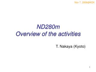
Overview of the read-out electronics for the TPCs at T2K ND280m P. Baron, D. Calvet, X. De La Broïse, E. Delagnes, F. Druillole, J-L Fallou,J-M. Reymond, E. Virique, E. Zonca DSM/DAPNIA/SEDI, CEA Saclay 91191 Gif-sur-Yvette Cedex, France
Plan • Context • TPC Read-out Architecture • Summary 2
TPC Configuration 3 TPC stations 2.5 m y z x 2.5 m Detector module 1 m • Features • 3 TPCs stations; each with 2 planes of 2 x 6 detector modules • Each detector module: Micromegas, 27-30 cm square • Module segmentation: 1728 pads of 9.7 mm x 6.9 mm • Total number of pads: 124.416 • 512 space points in z-axis, (2.5 mm spacing) 3
Outline of Requirements • Functional and Performance • Noise, dynamic range, resolution, linearity • SNR=100 (i.e. 700 e- rms for 12 fC MIP), 10 MIP on 12 bits, 1-5% • Event rate: ~0.3 Hz spill + cosmic. For DAQ: 20 Hz mean and max. • 512 space points, various gas: 14-500 µs drift (1.25 m drift distance) • Support for GEM and Micromegas charge amplification technology • Non Functional and Environmental • Compact, low power, modest magnetic field (0.2 T), no radiation • Underground experiment (Japan), fire and seismic safety rules • Demands on front-end electronics and data acquisition • Highly segmented detector (124 k channels) • Extreme burstiness of initial data (several Tbaud/s peak) • Large event size (90 MB) but modest event rate (few Hz) → Strategy: re-use ALTRO based electronics for detector R&D; while designing new read-out electronics 4
Complete Logical Read-Out Flow ~124.000 channels 1-6 Tbaud*/s peak 1728 Front end ASICs Pre-amp and shapers *1 baud = 10 bit ~2 ms retention max. Samplers and analog memory buffers 432 Front end cards 34 Gbaud/s peak Analog to digital conversion 400 Gbit/s peak On-detector electronics Digital buffer 72 Mezzanines 72 Optical fibers ~1-10 Gbit/s averaged Data concentration 6 Concentrator Cards Standard LAN connection(s) ~0.1-1 Gbit/s Shared DAQ system • Architecture principles • Front-end ASIC with analog memory (Switch Capacitor Array) • ADC + digital buffer mounted close to the detector • Multiple optical fibers send data to off-detector concentrators • Interface to common DAQ via standard network 5
Detector Module Read-out 1728-pad detector plane 288-channel analog Front-End Card (FEC) 80-pin connector 72-channel ASIC Slow-control network Quad-channel ADC digital Front-end Mezzanine card (FEM) FPGA Fiber to DCC Optical Transceiver Power bar Low-voltage power 72 modules in total 6
TPC Plane Readout Inside the Magnet Off-detector TPC plane 12 optical fibers Detector Module Front- End Card Front-End Mezzanine card Optical link Data Concentrator Card x 6 • 1 of 6 TPC planes shown – 3 TPC stations • 6 x 2 detector modules per TPC plane – 72 modules in total • 1 duplex optical readout fiber per detector module • 1 external data concentrator per TPC plane – 6 concentrators in total 7
TPC Event Building, DAQ Interface 6 concentrators Detector A VME/PCI backplane bus Common DAQ Run Control Network TCP/IP Gigabit Ethernet Commercial Linux PC Global Clock Trigger Detector B Detector TPCs • Principles • Event Building for TPC data over backplane bus with a PC or each concentrator send data directly to the DAQ via a LAN connection • Interface to common DAQ system via standard Gigabit Ethernet LAN • TPCs (like other detectors) compliant to the experiment wide physical interface specifications, protocols and software framework 8
X64 Asic T2K 1 channel BUFFER SCA FILTER GAIN ADC CSA 512 cells Tpeak;Gain TEST SCA MANAGER SLOW CONTROL Stop CK Serial Interface Trigger CK In Test Front-end ASIC Synopsis 9
SCA: 76x511 Cells Front-end ASIC: AFTER Technology: AMS CMOS 0.35mm Area: 7546mm x 7139 mm Submission: 24 April 2006 Delivered: end of July Package: LQFP 160 pins; Plastic dimensions: 30mm x 30mm thickness: 1.4mm pitch: 0.65mm Number of transistors: 400,000 AFTER : Asic For Tpc Electronic Read-out 10
Analog Front-end Card Connectors to detector plane Passive Components ASIC ASIC ASIC ASIC ~14 cm 4 channel ADC 288 channel FE card Digital output ~25 cm Features • 6 Analog Front-end cards per detector module; i.e. 432 cards in total • Throughput: 0.96 Gbps per card, 414 Gbps total • Plugs at the back of detector plane; inside the magnet – water cooling • Conceptual design in progress – first prototype expected Q2-Q3 2006 11
ASIC Test Card ZIF Socket Interface connector to FEM Features • Essentially FEC pre-prototype; 4 ASICs (1 socketed) • Board under assembly; expected in the next few days 12
Connector Evaluation: Detector R&D Prototype Micromegas Detector plane Protection Card The GEM and Micromegas detector R&D on HARP used the proposed connector on the protection card → Proposed connector is now validated 13
Digital Front-end Mezzanine Card Analog FE Card Analog FE Card Analog FE Card Analog FE Card Clock Trigger Control Data 1.2 Gbit/s peak ~5 Gbit/s ~5 Gbit/s Memory ~6 Mbit FPGA Logic Digital Front end Mezzanine Card ~12 Mbit/s Clock Trigger Control Optical Link Average rate < 50 Mbit/s Architecture • Commercial FPGA, memory and optical transceiver • Target: Xilinx Virtex-2 Pro / Virtex 4 with RocketIO transceiver • Design in progress – supports 4-6 FE cards • First prototype: end 2006; i.e. 6 months after number of FE card frozen 14
Reduced FEM card Architecture • Daughter card for a commercial Memec FPGA kit; can drive one FEC → Setup used for ASIC test, and prototype boards validation 15
Off-Detector Concentrator Card Optical transceivers Main data VME or PCI Slow control Main data 1-2 Gbit/s Slow control data FPGA logic Slow control commands Global clock Trigger Global clock Trigger • Principles • Standard form factor (6U or 9U); VME or Compact PCI backplane bus • Clock, trigger and control signals fanout, slow control interface 16
Integration, Resources • On-detector Electronics • Power supplies and power distribution, forced cooling; 3 kW • Common/shared services • Trigger generation • Global clock source and inter-detector synchronization • DAQ hardware interface and software • Slow control, configuration, monitoring • Racks, type of crate, common hardware/software platforms • Cooling water and heat exchanger • Resources for TPC electronics • ~30 FTE (Saclay, Lpnhe, Barcelona); investment: ~480 k€ • Planning • 1 TPC detector module equipped with prototypes in mid-2007 • Mass production of electronic cards and tests in 2008 • Installation and commissioning for operation in April 2009 17