Download
1 / 36
360 likes | 365 Views
Enhancing Electron Emission. Zeke Insepov, ANL. Outline. Introduction – Spicer’s Photoemission model Search for new PC materials Band structure of bi- and multi-alkali PC Electron emission enhancement Anti-reflecting coatings (Nanorod Arrays, Moth-eye concept) Electric field assisted PE

E N D
Enhancing Electron Emission Zeke Insepov, ANL
Outline • Introduction – Spicer’s Photoemission model • Search for new PC materials • Band structure of bi- and multi-alkali PC • Electron emission enhancement • Anti-reflecting coatings (Nanorod Arrays, Moth-eye concept) • Electric field assisted PE • MC simulation of pillar photocathode • MC simulations of MCP test experiment • PC lifetime, aging, ion feedback • Summary
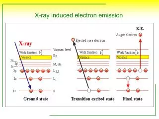
Introduction - Spicer’s model (1) (2) (3) VL Random walk with small loss due to collisions (~ 100 colls) la/Lis an important parameter Escape to vacuum Excitation PE can be approximated by a step function. Usually PE does not exceed 0.5. aPE - electrons are excited above the vacuum level (VL) and have possibility to escape,an is the absorption that does not produce yield. aPE/a1 for NEA la is the absorption length, L is the escape length. If L<< la, only a small fraction of the PE contributes to the yield. L can be obtained from experiment or by MC. [W. Spicer, Phys. Rev.112 (1958) 114]
Parameters for efficient PC • The photon absorption a=1/la, Ea, Eg : Search for new materials • The diffusion length L: • In UV region: la/L~ 104 • For semiconductors: la/L~ 1 • The escape probability PE • normally it is ~ 0.5 • For CsI : ~ 1 • For metals: < 0.1 • Field enhancement, band bending • (110)-Cs-O: DE=0.23eV (GaAs, [2]) • (110): DE=0.28eV • (111A)-Ga: DE=0.86eV, w = 155Å, PE=0.21 • (111B)-As: DE=0.1eV, w = 51Å, PE=0.49-0.58 • NEA [1] Spicer, slac-pub 6306 (1993) [2] James et al, J. Appl. Phys. (1971)
New PC material: Li2CsSb • Band structure, absorption coefficient of Li2CsSb were calculated via full potential linearized plane wave DFT-method [1]. • The direct vertical transitions generate photoelectrons. • After relaxation to X, and it can only recombine through an indirect annihilation process with a valence band hole in G. • DEG=1.05 eV, (red part) • DEC=0.68 eV • No barrier for GC • a = 35 mm-1 – calculation (la=285Å) [1] Ettema, Appl. Phys. Lett. (2003) [2] Niigaki, ibid (1999)
Diffusion and drift of carriers Drift, impact ionization [Insepov et al, Phys. Rev. A (2008)] Step2: Diffusion L depends on defects, dislocations, impurities. GaAs – L 1.2-1.6m for NZn=(1-3)1019 cm-3 Best GaAs PC [doped Ge]: L ~ 5-7 m[1] [1] Eden, Mall, Spicer, Phys. Rev. Lett. (1967) [2] James, Moll, Phys. Rev. 183 (1969)
EEE: Anti-reflecting coatings Tissue has a transparency window l=700-900 nm that can be used for detection of breast cancer. 45 times improvement factors for two S20 photocathode tubes resulting from waveguide coupling. • Improvements can be done due to strong dependence of the absorbance on the impact angle. • Surface cone design improve absorption • Half angles between 45 and 9 degrees give increase ~ 2 at 400 nm; • 8 times at 850 nm. Waveguiding in the PMP window, The full widths of the images are 60, 133 and 133 mm respectively. [Downey et al, Phys. Stat. Sol. (2005)]
EEE: Nanorod Array layers Fig. 1 • Planar Cd-(Se, Te) PE vs nanorod array : • Hi-aspect ratio nanorods could provide absorption along its axis, while collecting carriers radially (Fig. 1). • The spectral response of the nanorod array PE exhibited better QE for collection of near-IR photons. (Fig. 2) L ~ 1/a Fig. 2 charge Light [Spurgeon et al, 2008] • Solar cell’s antireflective and all-angle coating built by seven layers, with a height of 50-100 nm, made up of SiO2 andTiO2 nanorods positioned at an oblique angle, absorbs 96.21% of the spectrum from UV to visible light and IR, from all angles. [Rensselaer Polytech Inst]
EEE: Moth-eye concept • The surface of the moth eyes consists of an array of protuberances, termed corneal nipples. • The nipples are arranged in domains with hexagonal packing, the distances are from 180 to 240 nm, the nipple heights varied between 0 and 230 nm. • The nipples create an interface with a gradient refractive index between that of air and the lens material. • The reflectance progressively diminished with increased nipple height. Nipples with a paraboloid shape and height 250 nm, touching each other at the base, virtually completely reduced the reflectance for normally incident light. [Stavenga et al, Proc. R. Soc. B (2006)]
EEE: high electric field Internal electric fields: eNd db x -da -eNa • Poisson equation V(x) the potential, r the charge density, and e the dielectric constant External electric fields: E = 7.9105 V/m [1] E = 4 106 V/m [2] • E-field increases QE in IR • Negative effect - dark current [1] Crowe et al, Appl. Phys. Lett. (1967) [2] Coleman, Appl. Opt. (1978)
Field Enhancement: Si, GaAs • Electric field enhancement from NEA Si, GaAs was observed. • E increases the PE and does not change the spectral response of the NEA surface. • Surface potential lowering by the Schottky effect. External field E reduces the work function via Schottky equation: Band bending region: w=200Å Si : 51018 cm-3, 0.6 MV/m w=240Å GaAs : 71017 cm-3 [Howorth et al, Appl. Phys. Lett. 1973]
Field Enhancement: Alkali PC Gain Photon energy, eV • Cs2Te photocathode was studied • Schottky lowering explained the results for enhancement factor ~ 5. • E= 4 MV/m [2] • Trialkali (Cs)Na2KSb – the electric field was applied and the magnitude of QE increase from 3 to 6 times was observed with a maximum in l = 925 nm. • This is due to a lowering of the potential barrier at the vacuum interface. • Experiment [1]: • 1) E = 1.3 104 V/m • 2) E = 7.9105 V/m QE enhancement factor (ratio of high-field and low-field QE) as a function of wavelength. [2] Coleman, Appl. Opt. 1978 [1] Crowe et al, Appl. Phys. Lett. (1967)
Field enhancement: Multi-alkali • S20 and S25 photocathodes [Na2KSb(Cs)] • E=3 MV/m This is consistent with a Schottky explanation and the increase in photo yield with applied field was found to obey the Schottky equation. [Holtom, J. Phys. D (1979)]
MC study - Motivation • Nanostructured PC surface study – MC can recreate roughness, poly- or nano-crystalline, pillar, nipple, or other metamaterial types • Arbitrary doping, impurity and electric field simulation • Arbitrary barrier shapes and realistic escape probability • Testing various electron scattering models • All materials (metals, alkaline, semiconductors)
Transport of hot electrons in metals • Monte Carlo method was applied to the problem of “hot” electron motion in metals; • e-e scattering length, e-ph length and attenuation length was obtained. • Specular and diffuse reflectance at the boundaries were simulated. • Comparison with the theory for Au, Ag, Pd. Probability of e- excited at x reach the barrier with E By calculating the number of hot electrons crossing the barrier, for different sample thickness, the attenuation length L can be obtained. [Stuart, Wooten, Spicer, Phys.Rev.1964]
Physical model and parameters • (1) Photoexcitation of carriers – I(x)=I0 exp(-ax) • exponential law with a=7.7105 cm-1 (typical for Au) – can be adjusted for different materials; • Electrons are isotropically distributed in all directions • (2) Scattering of excited carriers; • e-e, e-ph scattering Eph kq (q - Debye temperature) • e-impurity/defect scattering (Brooks-Herring law) • (3) Escape of carriers over the barrier. • Elastic scattering interface (no energy change) • Lambert law in direction [Stuart, Wooten, Spicer, Phys.Rev.1964]
Algorithm of MC program • Initial source of electrons S(X,E) is created • E = EF + hn-(hn-ef)c1, 0c11 • Exp attenuation: X=T+(1/a)ln{1-c2[1-exp (-aT)}, • T– sample thickness, 0c21 • Collision simulation: lT=lelp/(le+lp) – the mean free path • Exp law: l=lT |ln c3|, 0c31 • Angle to normal: cos q = 2c4 -1, 0c41 (all dW are eq. probable) • c5 < lT/le,0c51 – choice for kind of collision • New electron, new trajectory, similar to previous • The process continued until the electron E < E0 • 10,000 trajectories computed for each sample; (statistics) • 200, 400, 600, 800 , and 1000Å samples were simulated • Specular reflection from the vacuum boundary [Stuart, Wooten, Spicer, Phys.Rev.1964]
MC simulation results • Quantum Yield vs thickness • Comparison of MC e-e mean free path le with experimental [1,2] and theory-I [2] and theory –II [2] with d-electrons. [1] Spitzer et al, Phys. Rev. (1962) [2] Quinn, Phys. Rev. (1962) Quantum yield vs thickness for specular reflectance. Each data point – 105 trajectories. [Stuart, Wooten, Spicer, Phys.Rev.1964]
Pillar structure Secondary electrons Glass window photon
Pillar simulation Cross-section of pillar Absorber (Al or GaAs), d ~ 50 nm Al absorber CsO, d ~ 10 nm TiO2 TiO2 primary electron TiO2 pillar E=2-5 V/mm Photon secondary electron CsO photocathode Low work-function coating (CsO), d ~ 10 nm Absorber (Al or GaAs), d ~ 50 nm TiO2 pillar ( ~ 50-200 nm) Z. Insepov, V. Ivanov
PC simulation parameters • Photon energy : 1.5-6.2 eV (800nm-200nm) 1.4eV • Kinetic energy of SEE: 0.5-5 eV • Electric field ~ 2-5 V/µm accelerates PE to 2.5-10 eV • Electric field geometry is being determined by the resistivity of PC: 100 MW (Comsol)
Pillar Simulation Geometry Z. Insepov, V. Ivanov
Angular dependence of Gain, TTS • At 45, the electron trajectories are switching from “crossing” to “hopping” mode. This reduces the TTS value. • At large angles, the number of collisions becomes higher and that reduces the Gain: SEE 1 at small energies. Z. Insepov, V. Ivanov
Gain and TTS vs pillar angle Switching to hopping mode
Time drift simulation for APS setup dCsI=120 nm [Experiment: M. Wetstein (ANL)]
APS experiments [Experiment: M. Wetstein (ANL)]
Space-Charge Effect in PC • The higher the number of cloud electrons per pulse Nc,the stronger is the space-charge effect. • Non-negligible space-charge effects occur already at rather low values of Ncof about 1000e per pulse [1]. • APS experiments have estimated Nc per pulse >> 1000e [2]. APS experimental data Q = Imax*t0=140mA*80 ps = 1.12 10-14 C Nc = 7104 electrons per pulse [2] [1] J. Zhou et al, J. El. Spec. Rel. Phen. 2005. [2] Matt Wetstein, ANL
Drift-diffusion model of electrons Drift+Diffusion model hn < Eg Laser beam Langevin equation Absorption length in CsI at l=220 nm la=22 nm[3] <v> E = U/d e-Escape length in CsI Vacuum [1] Breskin, NIMA (1996) [2] Aduev, Phys. Stat. Sol. B (1998) [3] Boutboul, J. Appl. Phys. (1998) L=16nm[1]
MC model of random walk CsI Ld – e-e + e-ph + e-defects La vacuum Ld z e E window [1] Boutboul, J. Appl. Phys. (1998) [2] Breskin, NIMA (1996) Photocathode
Random walk + drift E Ld=10 nm La=100 nm thick=120 nm m*=0.1m U=1-3.5 keV
Field dependence of TT d time v x E
Summary • Electron emission can be enhanced by various methods: nanostructured interfaces, doping and applying electric fields, multilayer coatings, NEA • Theory and simulation methods are not yet capable of treating complex PC tasks, such as surface roughness, nano-structured, real material properties, hot carriers and plasma effects, high electric fields in PC, aging • Nano-pillar PC structure was simulated and optimized • MC method is being developed to evaluate surface roughness, plasma and hot electrons effects, complex materials, high electric fields and photon fluxes.
Acknowledgments • H. Frisch, ANL • V. Ivanov, Muon Inc. • K. Attenkofer, ANL • A. Terekhov, Novosibirsk, Russia