Download
1 / 18
180 likes | 281 Views
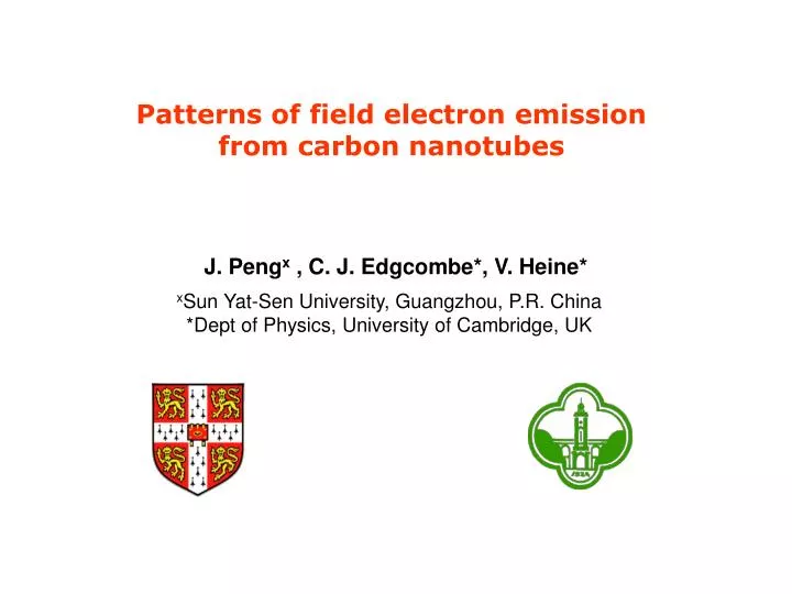
Patterns of field electron emission from carbon nanotubes . J. Peng x , C. J. Edgcombe*, V. Heine*. x Sun Yat-Sen University, Guangzhou, P.R. China *Dept of Physics, University of Cambridge, UK. +1000 V. vacuum. 0 V. CNT. ~10 mm. W. few nm. V. E. s. barrier. Introduction.

E N D
Patterns of field electron emission from carbon nanotubes J. Pengx , C. J. Edgcombe*, V. Heine* xSun Yat-Sen University, Guangzhou, P.R. China *Dept of Physics, University of Cambridge, UK
+1000 V vacuum 0 V CNT ~10 mm W few nm V E s barrier Introduction Experiment: Field emission microscopyof carbon nanotubes (CNTs) The pattern observed on screen sometimes1,2,3 consists of sets of dark-centred rings that together form a pentagon or hexagon, with fringes between adjacent rings.
Fig. 1 Hata et al (Ref. 3) Explanations have been proposed for the fringes2,3,4. The fact that the centres of the rings are dark, when simple interference theory suggests they should be bright, does not seem to have been explained hitherto.
Pentagons in the cap Formation of a closed cap on a carbon nanotube requires the presence of at least 6 pentagons of carbon atoms. The direction of the surface normal changes more rapidly near these pentagons than over the hexagons forming the rest of the CNT. Hence the local field and the induced charge density are greatest, and the potential barrier is thinnest, near the pentagons. Where the barrier is thinnest, the wave function is attenuated least. So the current density emitted from pentagons is likely to be much greater than from the rest of the CNT structure. Fig. 2 Hata et al (Ref 3) We interpret the individual rings seen in Fig. 1 as coming from different pentagons in the cap, distributed approximately as in Fig. 2. In a real CNT, the positions of pentagons may be distributed without exact symmetry.
Why does each ring have a dark centre ? The pairs of dark bands seen between adjacent rings suggest interference between waves associated with the pentagons. Thus the emission from adjacent pentagons seems coherent. Then we can expect wavefronts from all parts of a pentagon to travel the same distance to any point on its axis, so we might expect wavefronts to reinforce at the axis and produce the strongest current density on the axis. But the image shows that the centres of all rings are darker than the surroundings – that is, the current density on each ring axis is smaller than the density off-axis. How does this happen ?
Band structure for pentagons Each pentagon has bonds to surrounding atoms, but to simplify the description, the effect of neighbouring structure is ignored here; only the wave function of a pentagon is considered here. Symmetry and theory for a simple ring suggest that the wavefunctions of p orbitals on a pentagon have a regular phase variation around the axis that is non-zero above the ground state. For states varying as exp (imf), the relation between orbital energy and m is as shown in Fig. 3.
Fig. 3 Band structure for pentagon and occupation of levels In the absence of applied field, each pentagon has 5 p-electrons which fill the m = 0 states and some of the m = ±1 states of the possible orbitals. States described by exp ±imf can be combined to give real functions cos mf and sin mf. Emission from the states m = ±1 comes from a superposition of these functions and so the density is independent of f. Electrons can tunnel from states m = 0 and m = ±1, but because the m = 0 state is lower in energy, the potential barrier seen by an electron with m = 0 is both wider and higher than that seen by an electron with m = ±1. The density of m = 0 electrons is thus much more heavily attenuated by tunnelling than the m = ±1 density. The stream emerging from the barrier can thus be expected to contain mainly electrons with m = ±1.
Calculated electron density at the CNT apex In general it’s difficult to calculate a steady-state distribution of charge outside the CNT with DFT codes, since they show correctly that, under realistic emission conditions, the charge all falls to the anode. The code ONETEP allows charge to be confined by use of Wannier functions. This can represent the relatively high charge density in the barrier region while ignoring the smaller density outside it. Fig. 4 Surfaces of constant induced charge density (increasing l - r) for (18,0) nanotube with 6 pentagons at outer circumference, in applied field of 28 V/mm, calculated by DFT code ONETEP (Ref.5).
W V E s barrier Analysis using the complex wave function shows that the phase does not change much in the barrier region. Hence the relative phase of emission from different parts of the pentagon persists during an electron-wave’s travel through the potential barrier at the tube tip. Beyond the barrier the phase changes with k0 = (2emV(s))1/2/ h .
From potential barrier to anode Electron-wave propagation from the outside of the potential barrier to the anode can be described (1) approximately by optical theory; (2) approximately by ballistic theory; or (3) by solving Schrödinger’s equation. Optical theory is approximate since it assumes constant k0 = w / c. Realistically, the electrons start with low speed and have k0 ~ V(s)1/2, so their phase evolution differs from the optical model. Numerical solution of Schrödinger’s equation for realistic geometries is inaccurate, because the anode-cathode distance is very large compared with the required step length. However, Schrödinger’s equation can be solved analytically for some simple geometries.
Propagation from a ring in planar geometry We can find an analytic solution for a simplified geometry consisting of a circular emitting ring of radius a , in a planar cathode surface, subject to a uniform accelerating field F. The solution can be found for a general f-periodicity of the form eimf . Fig. 5 Emitting ring in planar geometry. The source is assumed to be y = d(r - a) at s = 0. axis
Assume y = R(r) Z(z) exp imf , with z = k2b2 - (s - s0) / b , b = (h2/ 2 m e F)1/3 ~ 3 Å , s0 = W/ e F, W = work function and F = electric field. The general solution of S’s eqn can be written in the form y = eimfò c(k) (Bi(z) + i Ai(z)) Jm(k r) k dk Here k is the phase constant for transverse (not axial) variation. The Airy functions Ai & Bi give well-defined solutions through V(s) - E = 0. Now y has the form of a Hankel transform, so can be inverted to define c(k), if the source distribution is known. With the assumed source condition y = d(r - a) at s = 0 (z = k2b2 + s0 / b), k is the phase constant for transverse (radial) variation.
The resulting amplitude of y at the anode varies with r as where m is the f-periodicity at the source, s is the anode-cathode spacing and V(s) is the voltage at s. Clearly y = 0 at r = 0 for all non-zero values of m . Only a small range of the radial phase constant k near zero contributes substantially to the result. This provides some justification for ignoring transverse variation in the conventional WKB approximation for the current transmitted through the barrier. The radial scale of the current density pattern at the anode increases as s and as V(s)-1/2. The result is like that for a ballistic particle with constant transverse velocity in a uniform axial field, but broadened.
So, when emission at the cathode is from a hollow ring, (1) when there is no phase variation around the emitting ring (m=0) then on axis (r = 0) the waves add in phase to give maximum charge density; (2) when the phase around the emitting ring varies with non-zero m, the charge density on axis at the anode is zero; (3) the pattern of current density distribution becomes broader as it moves away from the cathode. The observed pattern at the screen, with low intensity at the centres of rings, shows that little emission comes from m = 0 orbitals. The observed distribution seems consistent with m = 1 emission (transverse variation as J1(const . r)) .
Why is there coherence between pentagons ? In a CNT tip, the pentagons are separated by many bond lengths, and with such a large separation, it is not obvious that their wave functions should have a definite phase relation. However, the calculation of transit above shows that the principal contribution to the observed current comes from waves with very small transverse momentum, that is with k ~ 0. This means that electrons of the same energy will have the same axial momentum (at equal values of potential) and so phase relations existing on exit from the potential barrier will be preserved on transit to the anode. This may provide sufficient coherence for interference to be observed.
Some results of optical modelling (a) experimental current density distribution (Ref. 4); (b) result of modelling using optical rays, with single phase at source (Ref. 4); (c) result of modelling with optical rays, with one cycle of phase around each circular ring at source.
Conclusions 1. For a simple pentagon, available states have phase factors exp ±imf, where f is the azimuthal angle around the axis of the pentagon. Tunnelling and field emission can occur from states with m = 0 and ±1, but the current from m = 0 is more strongly attenuated by the larger barrier seen because it has lower energy. Thus the observed emission pattern is dominated by electrons from orbitals with phase factors exp ±if (or cos f and sin f). 2. The wave function calculated for charge accelerated from a ring in planar geometry shows a transverse variation at the anode as Jm(const x a r Va1/2 / s). Thus (in planar geometry) current from orbitals with m = 0 would have greatest density at r = 0, but current from orbitals with any other value of m has zero density on the axis. 3. The observed lower density at the centres of rings observed in Refs. 1 and 3 is consistent with emitted current coming mainly from orbitals with phase factor exp ±if, as expected for the Fermi level of a simple pentagonal ring.
Acknowledgments Thanks to Prof. R. Haydock and Dr. S. Kos for valuable discussions. References 1. Saito Y, Hata K & Murata T, Japan J Appl Phys 39 L271 (2000) 2. Oshima C, Matsuda K, Kona T, Mogami Y, Komaki M, Murata Y, Yamashita T, Kuzumaki T & Horiike Y, Phys. Rev. Lett. 88 038301 (2002) 3. Hata K, Takakura A., Miura K, Ohshita A and Saito Y., J Vac Sci Tech B 22, 1312 (2004) 4. Kruit P, Bezuijen M & Barth J E, J Appl. Phys. 99, 024315 (2006) 5. Skylaris C-K, Haynes P, Mostofi A & Payne M, J Chem Physics 122, 084119 (2005)