Download

1 / 36
420 likes | 673 Views
Memory and Register. Memory. terminology read/write operation volotile/non volatile determine the capacity from input and output timing requirements of ROM and EEPROM and Flash memory RAM and its organization Memory combinding. Memory layout in computer. high-speed memory for internal

E N D
Memory • terminology • read/write operation • volotile/non volatile • determine the capacity from input and output • timing requirements of ROM and EEPROM and Flash memory • RAM and its organization • Memory combinding
Memory layout in computer • high-speed memory for internal • low speed for external storage
Terminology • Cell : electrical circuit used to store a single bit data such as flip-flop circuit • Word: compound of bits • Byte: 8 bits word • Nibble: 4 bits word, half a byte • Capacity: • describe how many bits can store in a memory module • often show in (number of word x word size) form • 1K of cell = 210 = 1024 cells • 1M or cell = 220 • 1G or cell = 230 • Volatile memory • type or memory that always require electrical power unless data will lost.
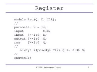
General memory signal and diagram • address lines corporate with address bus • data line corporate with data bus • control lines for memory operation type • R/-W read write operation, active low • ME : memory enable, active low • to enable the memory module • other name • /CS chip select • /CE chip enable • /OE : Output Enable: used to enable the RAM data to Data BUS
ROM – Read Only Memory • designed : holding permanent data / not change frequently • Data may enter during manufacturing process • Store microcomputer program because it is not volatile • also programmed and data such as calculator, appliances, security system etc.
ROM architecture • 4 basic part • row decoder • column decoder • register array • output buffer
Type of ROM • Mask-Programmed ROM • Programmable ROM (PROM) • Erasable Programmable ROM (EPROM) • Electrically Erasable PROM (EEPROM) • Flash Memory
Mask-Programmed ROM • program are written by manufacturer for custom specification • use photographic negative as mask to control electrically interconnection • mask is expensive thus need large quantity for economical cost • Cannot be reprogrammed • example use: ROM character generator for CRT
PROM • fusible-link MROM • custom programmed by user • OTP (One Time Programmable) properties: Once programmed, it cannot be erase.
Erasable Programmable ROM (EPROM) • When Program • need special voltage (typically 10-25V) • used amount time (typically 50 msec) • Erasable: by Ultraviolet (UV) light • examples • 2732 : 4K x 8 NMOS EPROM • 2764 : 8K x 8
Electrically Erasable PROM (EEPROM) • Erase by Electrically (high voltage) eg. 21v generated from 5v • Write faster than PROM (5usec) • During Write, internal circuitry automatically erases the cell • Former from Intel ex. 2816, 2864
Flash memory • high density than EEPROM • Faster erase and write time than EEPROM • 2 mode of erase • bulk erase: erase all cell • sector erase: specified part of cell to erase e.g. 512 bytes • typical 10 usec write time • example 28F256A
ROM applications • Firmware • data and program code while power up • Data table • constant data for look-up eg. store trigonometric tables • data converter • input one type output with another eg. input BCD code output with 7-segment code
Auxiliary Storage • Because of competitively cost some note book use as a small secondary storage • eg. thumb drive
RAM-Random Access Memory • Read/Write able memory • Volatile thus used as temporary storage or as registers • 2 kinds when divided by technology • Static RAM – Semiconductor RAM • Dynamic RAM – Capacitor RAM • size step from bytes, 1K, 2K, 4K…
RAM operation step • Set the address code at address bus • Activate /CS (Chip Select) • When Write • set Data to Data bus • R/-W set low • When Read • R/-w set high • Data comes out to data bus • /OE
Static RAM timing Read cycle Write cycle
Dynamic RAM • structure visualized as an array of single-bit cell
Each cell representation • data often referred the capacity to 1 cell e.g. 4096K x 1 for 1 bit word size, equals to 1024Kx4 (1Meg x 4) for 4 bit word size.
Address Multiplexing • Owing to its capacity is high, the require a lot of address lines • Multiplexing circuit is used to decrease number of address lines • add more control signal lines • CAS : Column Address Strobe • RAS : Row Address Strobe
Refreshing • Each memory cell has to be refresh periodically (typically 4 ms) or the data will be lost • Refresh performs when Read operation • By activate the ROW signal address, thus need more external or built in circuit • 2 refreshing mode • burst mode: normal operation is suspended, refresh contiguous row • distributed mode • intersperse with normal operation
when refresh • RAS is activate • CAS and R/-W are high
word size expanding • add more equal in size RAM module
Capacity expanding • need address select signal • often use the high+1 address line
Combining chips • need decoder, use the higher addresses line as decode signals