Download
1 / 71

E N D
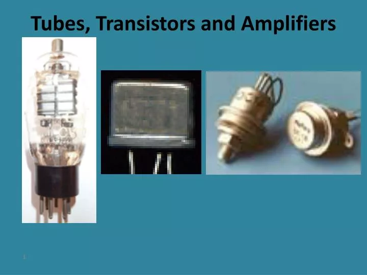
In 1947,Bardeen & Brattain at Bell Laboratories created the first amplifier!Shockley (boss), came near to canceling the project. The three shared a Nobel Prize. Bardeen and Brattain continued in research (and Bardeen later won another Nobel). Shockley quit to start a semiconductor company in Palo Alto. It folded, but its staff went on to invent the integrated circuit (the "chip") & to found the Intel Corporation. Interest
(+) Plate (-) Shield Control Grid (-) Cathode Inert Gas Heater Control Grid: Controls amplification rate & electron flow with bias voltage. Shield: Screen grid- increases electron speed cathode to + plate. Heater: Heats gas to gas amplification state. Inert Gas: Mercury or Argon gas. Tetrode Tube
Cathode Ray Tube (CRT) 3 Electron Beams (Red, Green, Blue) Phosphor Coated Screen Conductive Coating Grids (-) Cathode (+) Anode The cathode is a heated filament (like light bulb filament) in a vacuum inside a glass tube. The ray is a stream of electrons that naturally pour off a heated cathode into the vacuum. The + anodeattracts the electrons pouring off the cathode. In a TV's CRT, the stream of electrons is focused by a focusing anode into a tight beam and then accelerated by an accelerating anode. This tight, high-speed beam of electrons flies through the vacuum in the tube and hits the flat screen at the other end of the tube. This screen is coated with phosphor, which glows when struck by the beam.
History • Created in 1948 in the AT&T Bell Laboratories. • Scientists were performing doping experiments on semiconductor material (diodes) and developed a semiconductor device having three (3) PN junctions. Bipolar Transistors
NPN / PNP Block Diagrams Bipolar Transistor Construction Emitter Collector N P N Base Emitter Collector P N P Base
For any transistor to conduct, two things must occur. • Theemitter - base PN junction mustbe forward biased. • The base - collector PN junction mustbe reverse biased. Bipolar Transistor Theory
Bipolar Transistor Biasing (NPN) FB RB Collector - Emitter + N P N Base +
FB RB Bipolar Transistor Biasing (PNP) Emitter Collector - P N P + Base +
The + emitter repels the majority current carriers towards the emitter - base PN junction. • Majority current carriers pass through the forward biased emitter - base junction and flow into the base. Once in the base, these current carriers now become minority current carriers and are attracted to the strong negative voltage applied to the collector. • 90% of the current carriers pass through the reverse biased base - collector PN junction and enter the collector of the transistor. • 10% of the current carriers exit transistor through the base. • The opposite is true for a NPN transistor. Bipolar Transistor Operation (PNP)
The transistor below is biased such that there is a degree of forward bias on the base - emitter PN junction. • Any input received will change the magnitude of forward bias & the amount of current flow through the transistor. The magnitude of the output will be on the order of 1000x larger depending on the value of +VCC. Amplifier Operation +VCC RC + RB + Q1 0 0 Input Signal Output Signal
When the input signal is large enough, the transistor can be driven into saturation & cutoff which will make the transistor act as an electronic switch. • Saturation- The region of transistor operation where a further increase in the input signal causes no further increase in the output signal. • Cutoff- Region of transistor operation where the input signal is reduced to a point where minimum transistor biasing cannot be maintained => the transistor is no longer biased to conduct. (no current flows) Amplifier Electric Switch Operation
Transistor Q-point • Quiescent point: region of transistor operation where the biasing on the transistor causes operation / output with no input signal applied. • The biasing on the transistor determines the amount of time an output signal is developed. • Transistor Characteristic Curve • This curve displays all values of IC and VCE for a given circuit.It is curve is based on the level of DC biasing that is provided to the transistor prior to the application of an input signal. • The values of the circuit resistors, and VCC will determine the location of the Q-point. Amplifier Electric Switch Operation
IB IC 90 uA Transistor Characteristic Curve 80 uA 70 uA Q-Point Saturation 60 uA 50 uA 40 uA 30 uA 20 uA 10 uA 0 uA VCE Cutoff
When troubleshooting transistors, do the following: • Remove the transistor from the circuit, if possible. • Use a transistor tester, if available, or use a digital multimeter set for resistance on the diode scale. • Test each PN junction separately. ( A “front to back” ratio of at least 10:1 indicates a good transistor). Transistor Maintenance
Transistor Maintenance • This chart shows the readings for a good transistor. Transistor Maintenance Chart
Advantages of junction transistors over point contact transistors: • -Generate less noise. • -Handles more power. • -Provides higher current and voltage gains. • -Can be mass produced cheaply. Transistor Maintenance Chart
Questions Q) What is the 7 step troubleshooting method? A) Symptom recognition, symptom elaboration, list possible faulty functions, identify faulty function, identify faulty component, failure analysis, repair, retest. Q) What was the most difficult problem you ever troubleshot? A) Various
Amplifier Classification • Amplifiers can be classified in three ways: • Type (Construction / Connection) • Common Emitter • Common Base • Common Collector • Bias (Amount of time during each half-cycle output is developed). • Class A, Class B, Class AB, Class C • Operation • Amplifier • Electronic Switch Bipolar Transistor Amplifiers
Output Signal Flow Path Common Emitter Schematic +VCC RC + RB + Q1 0 0 Input Signal Output Signal Input Signal Flow Path
DC Kirchoff Voltage Law Equations and Paths +VCC Kirchoff Voltage Law Base - Emitter Circuit RC IBRB + VBE - VCC = 0 RB Collector - Emitter Circuit Q1 ICRC + VCE - VCC = 0
Positive Going Signal • Negative Going Signal + RC Common Emitter Operation 0 Base becomes more (+) WRT Emitter Input Signal RB FB IC VRC VC Q1 VOUT ( Less + ) + Base becomes less (+) WRT Emitter Output Signal FB IC VRC VC 0 VOUT ( More + )
Q1 Common Base Schematic Input Signal Flow Path RC RE RB + + CC 0 +VCC 0 Output Signal Flow Path
DC Kirchoff Voltage Law Equations and Paths Q1 Kirchoff Voltage Law Base - Emitter Circuit RC IBRB + VBE + IERE - VCC = 0 RE RB CC +VCC Collector - Emitter Circuit ICRC + VCE + IERE - VCC = 0
Q1 • Positive Going Signal • Negative Going Signal Common Base Operation Base becomes more (+) WRT Emitter RC RE RB FB IC VRC VC CC +VCC VOUT ( More + ) + Base becomes less (+) WRT Emitter FB IC 0 VRC VC 0 VOUT ( Less + ) Input Signal Output Signal
Output Signal Flow Path Common Collector Schematic +VCC RB + Q1 0 Input Signal + RE 0 Input Signal Flow Path Output Signal
DC Kirchoff Voltage Law Equations and Paths Kirchoff Voltage Law +VCC Base - Emitter Circuit IBRB + VBE + IERE - VCC = 0 RB Q1 Collector - Emitter Circuit ICRC + VCE + IERE - VCC = 0 RE
+VCC • Positive Going Signal • Negative Going Signal RB Base becomes more (+) WRT Emitter Common Collector Operation FB IE Q1 VRE VE VOUT ( More + ) RE Base becomes less (+) WRT Emitter + + FB IE 0 0 VRE VE Input Signal Output Signal VOUT ( Less + )
AZAZA VOPINI & House of BEC Common Common Common B E C Av = Voltage Gain Zo = Output Impedance Ap = Power gain Zin = Input Impedance Ai = Current Gain
Used to compensate for temperature effects which affects semiconductor operation. As temperature increases, free electrons gain energy and leave their lattice structures which causes current to increase. Transistor Bias Stabilization
Self Bias: A portion of the output is fed back to the input 180o out of phase. This negative feedback will reduce overall amplifier gain. • Fixed Bias: Uses resistor in parallel with Transistor emitter-base junction. • Combination Bias: This form of bias stabilization uses a combination of the emitter resistor form and a voltage divider. It is designed to compensate for both temperature effects as well as minor fluctuations in supply (bias) voltage. • Emitter Resister Bias: As temperature increases, current flow will increase. This will result in an increased voltage drop across the emitter resistor which opposes the potential on the emitter of the transistor. Types of Bias Stabilization
+VCC + Self Bias Schematic + + RC o o Initial Input Self Bias Feedback + RB Q1 o + VOUT = o Resulting Input
+VCC DC Component AC Component Emitter Bias Schematic RC + RB ++ + + Q1 o - o VOUT Initial Input + CE RE -
+VCC DC Component AC Component Combination Bias Schematic RC + RB1 ++ + + Q1 o o RB2 - VOUT Initial Input + CE RE -
The range or band of input signal frequencies over which an amplifier operates with a constant gain. • Amplifier types and frequency response ranges. • Audio Amplifier • 15 Hz to 20 KHz • Radio Frequency (RF) Amplifier • 10 KHz to 100,000 MHz • Video Amplifier (Wide Band Amplifier) • 10 Hz to 6 MHz Amplifier Frequency Response
Class ‘A’ Amplifier Curve IB IC 90 uA 80 uA 70 uA Saturation 60 uA 50 uA 40 uA 30 uA Q-Point 20 uA 10 uA 0 uA VCE Cutoff
Class ‘B’ Amplifier Curve IB IC 90 uA 80 uA 70 uA Saturation 60 uA 50 uA 40 uA 30 uA Q-Point 20 uA 10 uA 0 uA VCE Cutoff
Can be used for guitar distortion. Class ‘AB’ Amplifier Curve IB IC 90 uA 80 uA 70 uA Saturation 60 uA 50 uA 40 uA 30 uA 20 uA Q-Point 10 uA 0 uA VCE Cutoff
Class ‘C’ Amplifier Curve IB IC 90 uA 80 uA 70 uA Saturation 60 uA 50 uA 40 uA 30 uA 20 uA 10 uA 0 uA Q-Point VCE Cutoff
Direct: The output of the first stage is directly connected to the input of the second stage. Best Frequency Response - No frequency sensitive components. • Impedance (LC) Coupling: Similar to RC coupling but an inductor is used in place of the resistor. Not normally used in Audio Amplifiers. • RC Coupling: Most common form of coupling used. Poor Frequency Response. • Transformer Coupling: Most expensive form coupling used. Mainly used as the last stage or power output stage of a string of amplifiers. Amplifier Coupling Methods
+VCC2 Direct Coupling Schematic RC2 +VCC1 RB2 RC1 Q2 RB1 Q1
+VCC2 RC Coupling Schematic RC2 +VCC1 RB2 RC1 Q2 CC RB1 Q1
+VCC2 Impedance Coupling Schematic RC2 +VCC1 RB2 Q2 CC RB1 Q1
+VCC2 RC2 Transformer Coupling Schematic +VCC1 RB2 RC1 Q2 RB1 T1 Q1
Transistor Oscillators • . Tickler (Armstrong) Oscillator • . Schematic Diagram FEEDBACK L1 Q1 1 3 NPN C1 OUTPUT 2 4 RC T1 VCC CB RB RE CE
Tickler (Armstrong) Oscillator b. Physical Description • .) Uses an LC tuned circuit to establish the base frequency. • .) Feedback accomplished by mutual inductance coupling between the tickler coil and the LC tuned circuit. • .) Uses class “C” amplifier with self - bias. • . Operational characteristics • .) Output frequency relatively stable. • .) Output amplitude is relatively constant. • .) RF frequency range • .) Local Oscillator in receivers. • .) Source in signal generators. • .) Radio - frequency oscillators in the medium and high frequency range.
Hartley Series Fed Oscillator Schematic Diagram OUTPUT RB Q1 C1 C3 VCC L2 C2 RE CE L1
Hartley Series Fed Oscillator • .) Physical Description • .) Can generate a wide range of frequencies and is easy to tune. • .) Current Flows through the tank circuit in the series-fed, but not used in the shunt fed. • .) Operational Characteristics • .) Ordinary Operation: Class “C” amplifier with self-bias. • .) When output waveform must be constant voltage of a linear wave shape => Class “A” amplifier is used.
Hartley Series Fed Oscillator • .) Operation (Voltage applied to circuit) • .) Current flows from battery (VCC) through L3 from collector to emitter, through RE, through L1, and back to the battery. • .) The surge of current through coil L1 induces a voltage in L2 to start tank circuit oscillations. • .) When current first starts to flow through coil L1, the bottom of L1 is negative with respect to the top of L2. • .) The voltage induced into coil L2 makes the top of L2 positive. • .) As the top of L2 becomes positive, the positive potential is coupled to the base of Q1 via C1. • .) An increasing (+) on the base of Q1 causes forward bias to increase => IC increases => IE increases => IL1 increases and results in more energy being supplied to the tank circuit which in turn increases the (+) at the top of L2 and increases the forward bias on Q1.