Download
1 / 1
10 likes | 164 Views
Integrated Tests of a High Speed VXS Switch Card and 250 MSPS Flash ADC Hai Dong, Chris Cuevas, Doug Curry, Ed Jastrzembski, Fernando Barbosa, Jeff Wilson, Mark Taylor, Benjamin Raydo. I . Abstract

E N D
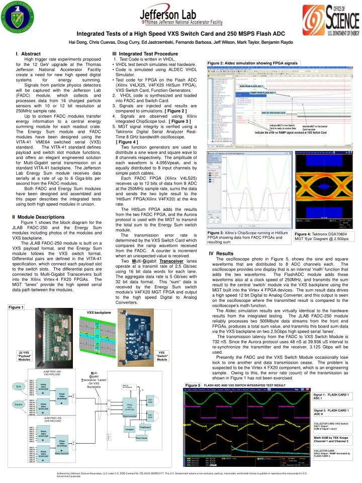
Integrated Tests of a High Speed VXS Switch Card and 250 MSPS Flash ADC Hai Dong, Chris Cuevas, Doug Curry, Ed Jastrzembski, Fernando Barbosa, Jeff Wilson, Mark Taylor, Benjamin Raydo I. Abstract High trigger rate experiments proposed for the 12 GeV upgrade at the Thomas Jefferson National Accelerator Facility create a need for new high speed digital systems for energy summing. Signals from particle physics detectors will be captured with the Jefferson Lab (FADC) module, which collects and processes data from 16 charged particle sensors with 10 or 12 bit resolution at 250MHz sample rate. Up to sixteen FADC modules transfer energy information to a central energy summing module for each readout crate. The Energy Sum module and FADC modules have been designed using the VITA-41 VME64 switched serial (VXS) standard. The VITA-41 standard defines payload and switch slot module functions, and offers an elegant engineered solution for Multi-Gigabit serial transmission on a standard VITA-41 backplane. The Jefferson Lab Energy Sum module receives data serially at a rate of up to 6 Giga-bits per second from the FADC modules. Both FADC and Energy Sum modules have been designed and assembled and this paper describes the integrated tests using both high speed modules in unison. • III Integrated Test Procedure • 1. Test Code is written in VHDL. • VHDL test bench simulates real hardware. • Code is simulated using ALDEC VHDL Simulator. • Test code for FPGA on the Flash ADC (Xilinx V4LX25, V4FX20 HitSum FPGA), VXS Switch Card, Function Generators. • 2. VHDL code is synthesized and loaded into FADC and Switch Card. • 3. Signals are injected and results are compared to simulations. [ Figure 2 ] • 4. Signals are observed using Xilinx integrated ChipScope tool. [ Figure 3 ] • 5. MGT signal integrity is verified using a Tektronix Digital Serial Analyzer Real-Time 8 GHz bandwidth oscilloscope. • [ Figure 4 ] • Two function generators are used to distribute a sine wave and square wave to 8 channels respectively. The amplitude of each waveform is 4.095Vpeak, and is equally distributed to 8 input channels by simple patch cables. • Each FADC FPGA (Xilinx V4LS25) receives up to 12 bits of data from 8 ADC at the 250MHz sample rate, sums the data and sends the two byte result to the ‘HitSum’ FPGA(Xilinx V4FX20) at the 4ns rate. • The HitSum FPGA adds the results from the two FADC FPGA, and the Aurora protocol is used with the MGT to transmit the total sum to the Energy Sum switch module. • The transmission error rate is determined by the VXS Switch Card which compares the ramp waveform received from the FADC. A counter is increment when an unexpected value is received. • Two Multi-Gigabit Transceiver lanes operate at a transmit rate of 2.5 Gb/sec using 16 bit data words for each lane. The aggregate data rate is 5 Gb/sec with 32 bit data format. This “sum” data is received by the Energy Sum switch module’s V4FX20 MGT FPGA and output to the high speed Digital to Analog Converters. Figure 2: Aldec simulation showing FPGA signals SUM FROM FLASH ADC 1 RAMP FROM FLASH ADC 2 DAC On VXS Switch Card II Module Descriptions Figure 1 shows the block diagram for the JLAB FADC-250 and the Energy Sum modules including photos of the modules and VXS backplane. The JLAB FADC-250 module is built on a VXS payload format, and the Energy Sum module follows the VXS switch format. Differential pairs are defined in the VITA-41 specification, which connect each payload slot to the switch slots. The differential pairs are connected to Multi-Gigabit Transceivers built into the Xilinx Virtex-4 FX20 FPGAs. The MGT “lanes” provide the high speed serial data path between the modules. Figure 3: Xilinx’s ChipScope running in HitSum FPGA showing data from FADC FPGAs and resulting sum Figure 4: Tektronix DSA70804 MGT ‘Eye’ Diagram @ 2.5Gbps IV Results The oscilloscope photo in Figure 5, shows the sine and square waveforms that are distributed to 8 ADC channels each. The oscilloscope provides one display that is an internal ‘math’ function that adds the two waveforms. The FlashADC module adds these waveforms also at a clock speed of 250MHz, and transmits the sum result to the central ‘switch’ module via the VXS backplane using the MGT built into the Virtex 4 FPGA devices. The sum result data drives a high speed 12 bit Digital to Analog Converter, and this output is seen on the oscilloscope where the transmitted result is compared to the oscilloscope’s math function. The Aldec simulation results are virtually identical to the hardware results from the integrated testing. The JLAB FADC-250 module reliably processes two 500Mbyte data streams from the front end FPGAs, produces a total sum value, and transmits this board sum data via the VXS backplane on two 2.5Gbps high speed serial ‘lanes’. The transmission latency from the FADC to VXS Switch Module is 732 nS. Since the Aurora protocol uses 48 nS at 39.936 uS interval to re-synchronize the transmitter and the receiver, 3.125 Gbps will be used. Presently the FADC and the VXS Switch Module occasionally lose lock to one another and data transmission cease. The problem is suspected to be the Virtex 4 FX20 component, which is an engineering sample. Owing to this, the error rate (count) of the transmission as shown in Figure 1 has not been exercised. Figure 1 VXS backplane (2) VXS “Payload” Modules VXS “Switch” Module JLAB FADC-250 VXS PAYLOAD Multi Gigabit Transceiver “Lanes” On VXS Backplane FPGA Xilinx XC4VLX25 ADC1 ADC2 ADC3 ADC4 ADC5 ADC6 ADC7 ADC8 Sine Figure 5 FLASH ADC AND VXS SWITCH INTEGRATED TEST RESULT FIFO (2) IDT72V36110 FPGA Xilinx XC4VFX20 12 + Signal 1: FLASH CARD 1 ADC 1 P0 DAC 5662 FPGA Xilinx XC4VFX20 FPGA Xilinx XC4VLX25 ADC9 ADC10 ADC11 ADC12 ADC13 ADC14 ADC15 ADC16 P3 Square + P4 Signal 2: FLASH CARD 1 ADC 8 + DAC 5662 Ramp Generator JLAB FADC-250 VXS PAYLOAD COLLECTOR CARD (VXS Switch) DAC1 Output : SUM of Signal 1 and 2 “ChipScope” FPGA Xilinx XC4VLX25 ADC1 ADC2 ADC3 ADC4 ADC5 ADC6 ADC7 ADC8 Compare PWR Error Count FPGA Xilinx XC4VFX20 Math SUM by TEK Scope Channel 1 and Channel 2 + P0 FPGA Xilinx XC4VLX25 ADC9 ADC10 ADC11 ADC12 ADC13 ADC14 ADC15 ADC16 + COLLECTOR CARD DAC2 Output : RAMP Generated by FLASH CARD 2. Ramp Generator + Authored by Jefferson Science Associates, LLC under U.S. DOE Contract No. DE-AC05-06OR23177. The U.S. Government retains a non-exclusive, paid-up, irrevocable, world-wide license to publish or reproduce this manuscript for U.S. Government purposes