Download
1 / 18
210 likes | 467 Views
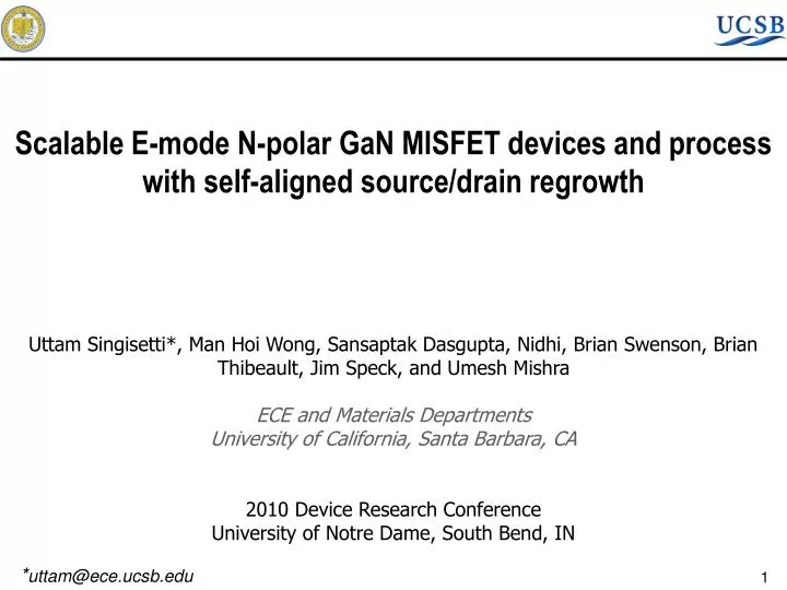
Scalable E-mode N-polar GaN MISFET devices and process with self-aligned source/drain regrowth. Uttam Singisetti*, Man Hoi Wong, Sansaptak Dasgupta, Nidhi, Brian Swenson, Brian Thibeault, Jim Speck, and Umesh Mishra ECE and Materials Departments University of California, Santa Barbara, CA

E N D
Scalable E-mode N-polar GaN MISFET devices and process with self-aligned source/drain regrowth Uttam Singisetti*, Man Hoi Wong, Sansaptak Dasgupta, Nidhi, Brian Swenson, Brian Thibeault, Jim Speck, and Umesh Mishra ECE and Materials Departments University of California, Santa Barbara, CA 2010 Device Research Conference University of Notre Dame, South Bend, IN *uttam@ece.ucsb.edu
Outline Motivation Why E-mode, N-polar Device design and Process Self-aligned device process E-mode device design Results Optical gate devices DC and RF data Conclusion and Future work
Why E-mode GaN devices GaN devices high speed and high breakdown high Johnston figure of merit D-mode HEMTs with ft ~ 200 GHz, fmax ~ 300 GHz Figure source: . T. Palacios group, MIT • Motivation for E-mode • Single voltage supply circuit • Simplified circuits • E-mode/D-mode logic circuits
Barrier N-face Ga-face Al(Ga)N GaN 2DEG 2DEG GaN buffer Al(Ga)N +++++++++++ Si doping GaN buffer Why E-mode, why N-polar GaN N-face EC VP EF GaN Scaling advantages of N-polar GaN AlGaN • Back barrier for electron confinement higher gm • No higher bandgap AlGaN layer on top low resistance contacts
Ga-polar E-mode devices with alloyed contacts Thinning down barrier under the gate Thicker barrier in the access regions Higashiwaki, IEEE TED 2006 F- on incorporation under the gate Thicker barrier in the access regions K.Chen, IEEE TED 2006 • Source/drain contacts to highband gap AlGaN layers • parasitic source contact resistance high Ron, gm degradation, scaling issues
Self-aligned scaled E-mode devices Figure source: . T. Palacios group, MIT Ultra scaled GaN devices: ft, fmax > 200 GHz • Self-aligned InGaN grade/InN source/drain to reduce access resistance* • Sub 100 nm gate-lengths velocity overshoot • Vertical scaling of channel to keep high aspect ratio * S.Dasgupta, APL 2010. Nidhi, IEDM 2009
20 nm channel Top AlN depletes 2-DEG under gate Under gate Under sidewall AlN removed under sidewall Under S/D contacts* * S.Dasgupta, APL 2010. Nidhi, IEDM 2009 Device structure and design
Device fabrication process * * U.Singisetti, pss(c) 2009, EDL 2009.
Selective AlN etch on GaN channel ∫ n(x) dx = 3×1012 cm-2 Band diagram after AlN etching • Digital etch 5 m UV ozone oxidation, BHF etch • 2 nm AlN etched in 4 cycles of etching • XPS on process monitor shows removal of AlN • Hall measurement gives ns = 3x1012 cm-2, agrees well to simulation No Al signal after etching XPS of process monitor sample
DC characteristics of E-mode devices Imax = 0.2 A/mm for Lg = 10 mm device Imax = 0.6 A/mm for Lg = 1 mm device
DC characteristics of E-mode devices Imax = 0.7 A/mm Vth • Vth = 0.8 V at Vds = 4.0V • Imax = 0.7 A/mm, gm = 250 mS/mm at Vds = 4.0 V • Imax = 0.22 A/mm, peak gm = 125 mS/mm at Vds = 0.5 V
Low gate leakage Maximum gate leakage current of 7 mA/mm at Vgs=5 V, and Vds =4.0 V
0.23 mm gate length device • Device no longer E-mode at Lg = 0.23 mm • Imax = 0.9 A/mm, peak gm = 210 mS/mm at Vds = 4.0 V
Short channel effect Threshold voltage decreases with drain bias (Vds)
Short channel effect • Vth roll off with gate length • Device becomes D-mode at Lg= 0.23 mm because of low aspect ratio (Lg/t = 230 nm/ 27 nm = 8.5) • Short channel effect is because of low aspect ratio and self-aligned access regions Need more vertical scaling for sub-100 nm E-mode devices
Device access resistance No InN Rs + Rd = 2 W-mm • Source access resistance of 1 W-mm, regrowth Rsh = 1000 W/□, Rc = 0.2 W-mm, high compared to D-mode devices* • Reasons: • Unintentional grading to In0.3Ga0.7N instead of In0.6Ga0.4N Higher sheet resistance • No InN coverage due to uncalibrated growth temperature Higher Rc • Rs can be easily reduced * S.Dasgupta, APL 2010. Nidhi, IEDM 2009
Conclusionsand future work • Scalable self-aligned N-polar E-mode devices • Vth = 0.8 V for Lg = 0.55 mm device • High current drive > 0.7 A/mm • Peak gm = 250 mS/mm • Short channel effects observed Future work • Vertical scaling and gate length scaling • Optimized regrowth